Nanoscale structures such as quantum wires and quantum dots are being researched widely with the aim to develop more remarkable devices, such as efficient LEDs and lasers, or quantum data processing components. One material that is being studied consists of semiconductor quantum wires based on InAs. This material is being studied as it has near-infrared optical properties.
Dr Benito Alén and co-workers on primary studies of isolated InAs nanowires have been involved in research that identifies novel behavior centered around the metal-insulator transition in correlated electron systems. They utilized NIR photoluminescence (NIR-PL) to investigate the transition dependencies on both temperature and excitation power.
NIR Photoluminescence
The investigation of the photoluminescence of individual semiconductor quantum wires is a crucial tool to test the function of attractive and repulsive Coulomb interactions among holes and electrons confined to one dimension. In these systems, the optical and electronic properties vary greatly based on the number of trapped carriers. However, the effect on the emission spectrum can be blurred if several QWRs with varying sizes contribute to the emitted light.
To determine the physics behind and tackle the experimental data against current theories, the photons released from a single QWR have be analyzed using high sensitivity light detectors and high spatial resolution methods. This technique has been demonstrated for InAs/InP QWRs emitting at 1.5 µm by a team of researchers in Spain at the Consejo Superior de Investigaciones Científicas (CSIC) and the Universidad de Valencia.
The estimation of low threshold for laser emission, slow surface recombination velocity, and decreased temperature sensitivity has greatly motivated the research on III-V semiconductor QWRs for optoelectronic applications. Among them, self-assembled InAs/InP QWRs can obtain their natural emission tuned beyond 1.6 µm and their areal density decreased to a few QWRs per square micron.
InAs/InP QWRs are suitable candidates for the fabrication of sophisticated light sources in the telecom spectral region, and for the research of new semiconductor physics. As for the latter, combined phenomena of 1D excitons have been analyzed in these nanostructures using NIR microphotoluminescence (µ-PL) methods at low temperature, at the Universidad de Valencia and published by B. Alén et al. in Physical Review Letters
The system is made up of a fiber-based confocal microscope embedded in the exchange gas chamber of an immersion liquid He cryostat. Excitation light from a 950 nm diode laser was focused into the microscope via a single mode optical fiber, whose core served as the excitation pinhole.
The laser light was aimed onto the sample via an objective lens (NA=0.55) generating a diffraction limited spot at the excitation wavelength. Light released by the few QWRs present in the excitation spot (AFM image in Figure 1) was gathered by the same objective and centered onto a diverse optical fiber, which was joined at its opposite end to a spectrometer fitted with a TE cooled Andor iDus InGaAs (DU490A-1.7) camera.
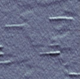
Figure 1. AFM image of the investigated QWRs (Courtesy Dr B Alén, CSIC, Madrid)
The faint light discharged from each QWR could be identified using exposure times of 10 to 100 seconds due to the low dark current of the cooled array and multichannel detection capacity of the iDus InGaAs array. The samples were prepared using self-assembly techniques of epitaxially growing InAs structures on InP (001) substrates under conditions that resulted in the formation of QWRs instead of quantum dots (QDs).
The aspect ratio and morphology of the individual QWRs were characterized using atomic force microscopy (AFM) and reflection high energy electron diffraction (RHEED) analysis. Usually these structures measured 20 nm in width and 200 nm in length, corresponding to aspect ratios of ~1:10.
Experiments were conducted to test how the samples behaved with variation in the excitation power, with powers down to 8 mW and up to 260 mW. The team also analyzed the temperature dependence.
Figure 2 shows typical examples of µ-PL spectra gathered on a single QWR as a function of excitation power density. The different-sized QWRs can discharge at different energies due to the quantum confinement size effect, but these QWRs reveal a similar trend with the growing photo-generated carrier density.
The analysis of the line shape of numerous spectral features noticed at low and high excitation allowed a comprehensive study of the metal-insulator transition controlled by improved Coulomb correlations in these systems.
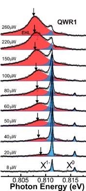
Figure 2. Typical single QWR emission spectra measured at 5 K with increasing excitation power. (Courtesy Dr B Alén, CSIC, Madrid)
At decreased powers, the sharp spectral feature at ~0.812 eV (~1528 nm) dominated, and at increased powers the wide spectral feature centered at ~0.807 eV (~1538 nm) dominated. This alteration in PL emission, caused by modifications in carrier density, indicates the metal-insulator transition. The spectra demonstrate that the insulating excitonic gas condenses into a metallic-like electron-hole liquid phase, with a spurt in carrier density.
Conclusion
Alén and team clearly showed the innovative behavior on the metal-insulator transition within a correlated electron system, as accomplished in single InAs/InP QWRs emitting in the NIR. They formulated methods based on µ-PL, which enabled the exploration of the carrier interactions and its reliance on photo-excitation powers and temperature. These primary studies will strengthen future developments of even more unusual devices, such as highly efficient micro-/nano- lasers and LEDs.

This information has been sourced, reviewed and adapted from materials provided by Andor Technology Ltd.
For more information on this source, please visit Andor Technology Ltd.