Nov 19 2009
Two-dimensional carbon layers, so-called graphenes, are regarded as a possible substitute for silicon in the semiconductor industry. The electronic properties of these layers can be varied by "building in" specific arrays of holes in their structure. Physicists at Empa, Switzerland, together with chemists from the Max Planck Institute for Polymer Research in Mainz, Germany, have, for the first time, succeeded in synthesizing a graphene-like porous polymer with atomic accuracy.
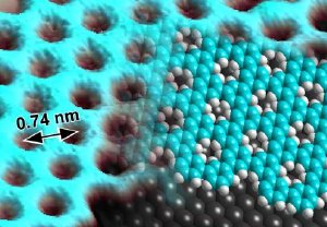
 Scanning tunneling microscope image of the two-dimensional porous polymer (left side of image) with a model of the material structure superposed (right side: blue-green - carbon; white - hydrogen; gray - silver surface).
Graphene consists of a two-dimensional carbon layer in which the carbon atoms are arranged on a hexagonal lattice, resembling a honeycomb. Carbon nanotubes are rolled-up sheets of graphene, and thick piles of graphene sheets form graphite.
Graphene boasts some very special characteristics - it is extremely tear-resistant, an excellent thermal conductor, and reconciles such conflicting qualities as brittleness and ductility. In addition, graphene is impermeable to gases, which makes it interesting for applications involving air-tight membranes. Because of its unusual electronic properties graphene is viewed as a possible substitute material for silicon in semiconductor technologies.
By inserting holes of a specific size and distribution into graphene sheets, it should be possible to impart the material particular electronic characteristics. For these reasons intensive research is being conducted worldwide into the synthesis and characterization of two-dimensional graphene-like polymers. Graphene and graphene-like polymers are currently hot research topics in materials science, with this year’s Körber European Science Award being awarded to the Dutch physicist Andre Geim for his pioneering studies in the field of two-dimensional carbon crystals.
New manufacturing method: “bottom-up” synthesis on metal surfaces
Together with colleagues from the Max Planck Institute for Polymer Research in Mainz, scientists from Empa’s “nanotech@surfaces” laboratory have for the first time succeeded in synthesizing a graphene-like polymer with well defined pores. To achieve this feat the researchers allowed chemical building blocks of functionalized phenyl rings to “grow” spontaneously into a two-dimensional structure on a silver substrate. This created a porous form of graphene with pore diameters of a single atom and pore-to-pore spacings of less than a nanometer.
Until now, porous graphene has been manufactured using lithographic processes during which the holes are subsequently etched into the layer of material. These holes are, however, much larger than just a few atoms in diameter. They are also not as near to each other and significantly less precisely shaped as with the “bottom-up” technique based on molecular self-assembly developed by the Empa and Max Planck group. In this process the molecular building blocks join together spontaneously at chemically defined linking points to form a regular, two-dimensional network. This allows graphene-like polymers to be synthesized with pores which are finer than is possible by any other technique.