Feb 6 2017
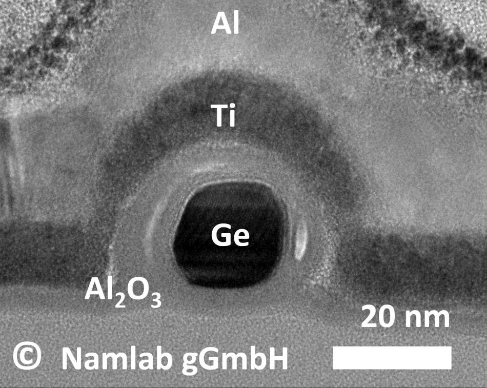
 Energy-efficient germanium nanowire transistor with programmable p- and n- conduction is shown. Transmission electron microscope image of cross section. CREDIT: NaMLab gGmbH
The first transistor based on germanium capable of being programmed between electron- (n) and hole- (p) conduction was demonstrated by scientists from the Nanoelectronic Materials Laboratory (NaMLab gGmbH) and the Cluster of Excellence Center for Advancing Electronics Dresden (cfaed) at the Dresden University of Technology.
It is possible to operate transistors based on germanium at reduced power consumption and low supply voltages because of the low band gap compared to silicon. Additionally, it is also possible to reconfigure the realized germanium based transistors between electron and hole conduction depending on the voltage applied to one of the gate electrodes. This allows realizing circuits with lower transistor count compared to modern CMOS technologies.
The currently existing digital electronics are dominated by integrated circuits constructed by transistors. For over four decades, transistors have been miniaturized to improve computational power and speed. The latest developments focus on maintaining this trend using materials with higher mobility than silicon in the transistor channel, like indium-arsenide and germanium.
One limitation in using those materials refers to the higher static power loss in the transistor’s off-state, also originating from their tiny band gaps. This issue was successfully solved by the scientist team around Jens Trommer and Dr. Walter Weber from NaMLab in collaboration with cfaed. This team conceived the germanium-nanowire transistor with separate gating regions.
For the first time the results demonstrate the combination of low operation voltages with reduced off-state leakage. The results are a key enabler for novel energy efficient circuits.
Dr. Walter Weber, Head of cfaed's Nanowire Research Group
This work has been featured in the journal ACS Nano.