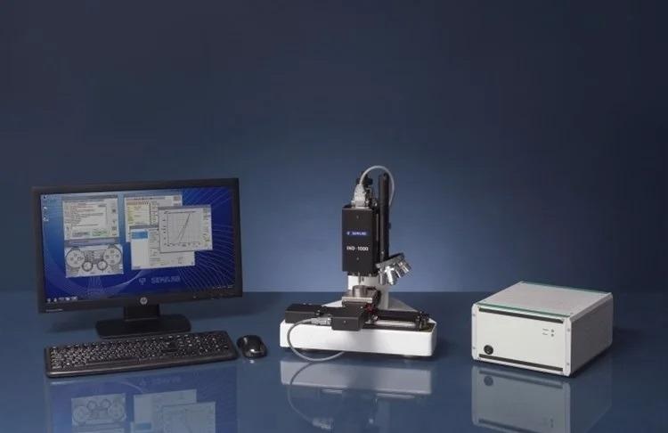
Nanoindentation is crucial for disclosing the quantitative mechanical properties of small volumes of materials. This method is currently a standardized technique for establishing elastic, plastic and visco-elastic properties of materials like soft films, ceramics, multi-phase metals, biological materials hard thin films, semiconductors and plastics on a micron to nanometer scale.
Nanoindentation Test
Precision load-displacement curves are provided by a nanoindentation test for use on both hard and soft surfaces. They can also be used on rough surfaces like those deposited by industrial processes. These processes include the formation of thermal spray coatings via quantitative measurement of the mechanical properties of small volumes of materials.
Thin films and biological materials are the main applications for such instruments apart from other applications, multi-phase metals and ceramics. Yet, they can also be employed for visco-elastic measurements of polymers, flexure testing of MEMS and any application which involves mechanical measurement on the sub-micron scale.
The material properties which can be measured are elastic modulus, yield strength and hardness, and depending on the sample, storage and loss moduli, fracture toughness, scratch and wear properties.
IND-1000
The IND-1000’s design enables it to apply a controlled load and deformation of the material under test. Displacement and force sensors are utilized for measuring the mechanical response of the materials.
The resolution and range of the actuator, force and displacement sensors are extremely small (in the μm and mN range with nm and nN resolution). The precise nature of the measurement allows the recording of events on the micro- to nanoscale.
Macro-scale damage can be clarified and elucidated by events on the sub-micron scale as a result. This enables the study of the basic properties of the sample and permits the properties to be customized for certain applications.

Image Credit: Semilab Semiconductor Physics Laboratory
IND-1000 uses robust LVDT sensors for both force and depth measurements. In this advanced package, AC amplification provides a millivolt noise floor. By offsetting the signal with the help of a special circuitry the full range of the analog-to-digital interface can be used.
CSIRO pioneered the use of the LVDT measurement sensors for nanoindentation applications in the late 1980s. Since then the method has been proven to provide a highly robust package and low noise sub-nanometer resolution.
Whilst competitor instruments employ a capacitance sensor, the IND-1000 system is almost resistant to mechanical breakage because of the overloading of the indenter shaft. This is because the indenter shaft passes right through the sensor and can withstand several millimeters of accidental deflection without any problem.
The force sensor is completely isolated from the load actuator and can measure the force applied to the indenter directly without any attenuation of the signal from the support springs.
The depth and force sensors are calibrated independently using international standards. It is possible to choose the closed loop feedback either from the depth sensor or from the force sensor. For high speed data acquisition the open-loop operation mode can also be selected.
Benefits
- Precise sample positioning can be guaranteed by video microscope and automated X-Y-Z-movement
- Sub-nanometer depth resolution and highly linear response LVDT
- Traceable calibration
- Almost resistant to mechanical breakage
- Robust design to endure considerable abuse
- Material properties like elastic modulus, yield strength, storage and loss moduli, hardness, fracture toughness, scratch and wear properties can be measured (based on the sample)
- The technology is based on the successful nanoindentation system of Fischer-Cripps Laboratories
- High quality PZT expansion element, without heat generation
- Closed-loop force/depth feedback
- Reliable performance for a number of years
- Low compliance enclosure, load frame and mountings
- Periodic calibration is not required
- Easy indenter tip changeover
- Real-time feedback control over application of depth- or load-independent force and displacement measurement
Optional Features
- Integrated finite-element analysis module
- Atomic force microscope
- Lateral force (scratch testing module)

This information has been sourced, reviewed and adapted from materials provided by Semilab Semiconductor Physics Laboratory.
For more information on this source, please visit Semilab Semiconductor Physics Laboratory.