Photothermal AFM-IR, or AFM-IR, is an analytical method used for chemical identification in a materials sample at the nanoscale. AFM-IR incorporates both the nanoscale spatial resolution of atomic force microscopy and the chemical analysis capabilities of infrared spectroscopy.
Compared to other nanoscale spectroscopic methods, such as scattering scanning nearfield optical microscopy (s-SNOM) and tip-enhanced Raman spectroscopy (TERS), AFM-IR can deliver a series of advantages, as it is easy to interpret and user-friendly with rapid measurement speeds and good data repeatability.
When running an AFM-IR spectrum, the results and rapid accumulation of point spectra for hyperspectral imaging can be achieved in two minutes. The AFM-IR technique can achieve sub-10 nm spatial resolution while establishing good monolayer sensitivity at various probing depths.
However, a variety of experimental factors can influence IR band intensities, positions, and shapes, and should be taken into account when interpreting AFM-IR spectra. This article highlights what photothermal AFM-IR can do and the various factors that can influence spectral interpretation.
What is Photothermal AFM-IR?
Atomic force microscopy is traditionally used for high-resolution imaging of materials samples to capture topographic, mechanical, and electrical properties, among others. In isolation, this method can achieve a spatial resolution of <10 nm using a sharp tip, and in some cases resolves at the molecular and atomic scale.
Comparatively, infrared spectroscopy can identify chemical species in materials exceptionally well, since each material has individual characteristic absorption bands in the “fingerprint” region due to distinct molecular vibrations.
When applying both methods simultaneously, AFM-IR can achieve chemical identification in a material with a spatial resolution several orders of magnitude less than the optical diffraction limit, which generally has a value of several to multiple tens of microns for a mid-infrared source.
AFM-IR is user-friendly compared to other nanoscale infrared spectroscopy techniques, most prominently scattering scanning near field optical microscopy (s-SNOM) and tip-enhanced Raman spectroscopy (TERS). Additionally, the AFM-IR spectra have a higher correlation with FTIR spectra.
AFM-IR can measure the cantilever oscillation signal, which is equivalent to the infrared absorption by the sample. By comparison, the long-established technique to measure a sample’s complex optical properties, s-SNOM, requires more intricate interferometric detection systems that rely on theoretical modeling. This can cause peak shifts in spectra as well as band shapes and peak ratios that are inconsistent when compared to the FTIR spectrum.1
Raman spectroscopy is a renowned analytical technique with the power to conduct molecular identification and structural analysis. The Raman scattering process has an exceptionally low cross section, especially where vibrations involving light elements are concerned. Moreover, it is dependent on the manufacturing of field-enhancing tips for TERS. This leads to limitations in consistency and reproducibility. Also, TERS captured from protein molecules are known to be lacking where amide bands are concerned, which limits their usability for determining protein secondary structure.2
AFM-IR differentiates itself from s-SNOM and TERS as it has a close correlation with transmission FTIR spectra in relation to peak shapes, band ratios, positions, and high signal-to-noise ratios.
History of AFM-IR Technology
First developed by Alexandre Dazzi, the AFM-IR technique leverages a “bottom-up” configuration,3 and commercial instrumentation based on Dazzi’s technique (nanoIR™) was first developed in 2010 by Anasys Instruments and subsequently acquired by Bruker in 2018.
There has been rapid progress in recent years as AFM-IR capabilities demonstrate improvements related to sensitivity, spatial and spectral resolutions, measurement time, and fields of applications.
Newer versions of nanoIR instruments (nanoIR2™, nanoIR3™) assumed a “top-down” configuration, which significantly improves the variety of samples that can be studied as they do not require an IR-transparent substrate.
Based on Bruker’s industry-leading Dimension Icon® AFM platform, the Dimension IconIR™ system is the most sophisticated, highest-performance AFM-IR instrument in the world today as a result of its low noise and high stability of AFM, high sensitivity and numerous modes of AFM-IR measurement. This is backed up by the availability of correlative studies concerning mechanical, electrical, and thermal properties.
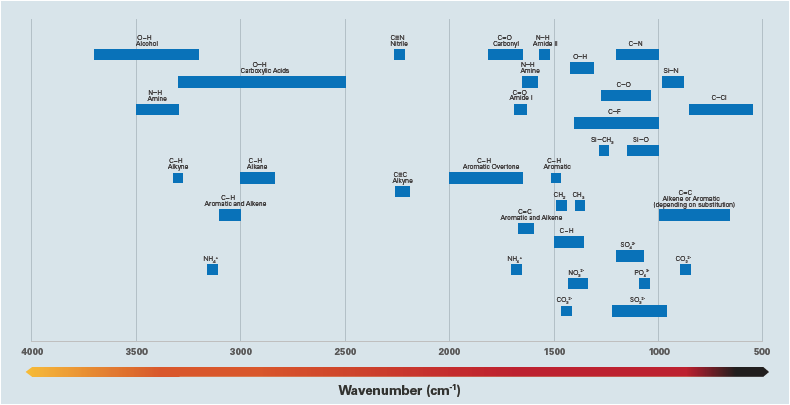
Figure 1. Typical IR absorption frequencies for common functional groups. Image Credit: Bruker Nano Surfaces and Metrology
Working Principles
AFM-IR uses an AFM tip to detect a sample’s local thermal expansion depending on its absorption of infrared radiation at the tip location. As a result, this generates a spatial resolution on the scale of the AFM tip radius. To achieve AFM-IR measurements, a region of a sample in proximity to the AFM tip is selected, and an infrared laser beam is concentrated onto the area.
When the infrared beam is absorbed, the sample instantly expands, consequently triggering a transient force on the AFM cantilever that propels it into oscillation.
The cantilever oscillation may stretch over various combined oscillatory eigenmodes as in conventional AFM-IR mode, or via a selectively enhanced individual eigenmode as in Resonance-Enhanced or Tapping AFM-IR modes.
AFM-IR spectra are captured by measuring the AFM cantilever oscillation amplitude as a function of wavelength while keeping the AFM tip fixed at xy positions on the sample. AFM-IR maps that show how chemical species are distributed across a sample are produced by scanning the sample while illuminating it with fixed wavelengths.
Hyperspectral imaging has become more commonplace with the advancement of measurement speeds, enabling comprehensive measurements of the AFM-IR spectra across a dense grid of points. This supplies precise information regarding molecular species and their distributions in the sample.
For an AFM-IR experimental setup, a pulsed laser source in combination with optics for beam steering, focusing, and polarization control are required.
A sample xy scanner is used to make sure the laser remains aligned with the tip. Even with a small temperature increase (<10 K with OPOs; <1 K with QCLs) and a regular thermal expansion coefficient (10-6 to 10-4), the resulting photothermal expansion is on the scale of several to tens of picometers for a polymer sample with a thickness of hundreds of nanometers.
The rapid speeds of the sample thermal expansion impact the instantaneous equilibrium position of the cantilever. This provokes the conversion of the thermal expansion on the scale of tens of picometers into cantilever oscillations on the nanometer scale. With improvements in sensitivity, the AFM-IR technique can now identify a single monolayer sample with a significantly lower thermal expansion.
The physics of how AFM-IR works is well-researched and relatively simple. The overall AFM-IR signal intensity as a result of the infrared absorption by the sample at the tip location is expressed in the equation shown below:4,5
| SAFM-IR ∝ HAFM Hexp Iinc (λ) α(λ) |
EQUATION 1. |
where HAFM and Hexp are contributed via the AFM cantilever oscillation dynamics, and the sample thermal expansion coefficient, Iinc (λ) is the laser power at the tip, and α(λ) = 4πκ(λ)/λ is the sample absorption coefficient shown at the wavelength λ with κ(λ) as the hypothetical part of sample refractive index.
From the above equation, while the intensity of the AFM-IR signal is dependent on other material properties of the sample, including thermal expansion coefficient and mechanical stiffness, these properties remain constant at a certain point on the sample, so they do not intervene with the relative peak intensities or peak shapes.
Therefore, the AFM-IR signal measured as the oscillation amplitude of the cantilever at a fixed point (X0, Y0) on a sample is relative to the absorption coefficient:
| SAFM-IR (X0, Y0) ∝ α(λ, X0, Y0) |
EQUATION 2. |
Moreover, the AFM-IR spectrum relates directly to the bulk FTIR spectra obtained in transmission mode. This approach lays the foundation for applying AFM-IR as a nanoscale chemical identification technique, as the AFM-IR spectra can be digitally cross-referenced against FTIR spectra on commercial databases and otherwise identified like any traditional transmission FTIR spectrum.
AFM-IR spectra agree with transmission FTIR spectra for a wide array of materials. Below is the comparison of an AFM-IR spectrum pulled from a polystyrene film of 300 nm thickness to an FTIR transmission spectrum.
The spectra show high correlation in both the CH-stretching region (2800-3200 cm-1) and the fingerprint region (1000-1800 cm-1).6,7 This underscores the power of AFM-IR spectroscopy as a chemical identification technique on the nanometer spatial scale, which surpasses the known capabilities of conventional FTIR instrumentation.
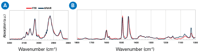
Figure 2. Comparison of AFM-IR and bulk FTIR spectra of a polystyrene film: (a) CH-stretching region, (b) fingerprint region. Image Credit: Bruker Nano Analytics
Major Operational Modes
Since the development of the AFM-IR technique, Bruker and its collaborators have produced several new AFM-IR modes, including Resonance-Enhanced, Tapping AFM-IR, PeakForce IR, and Surface Sensitive modes. Each mode has demonstrated exceptional strengths and has improved AFM-IR capabilities considerably, this has facilitated a number of breakthroughs in different research fields.
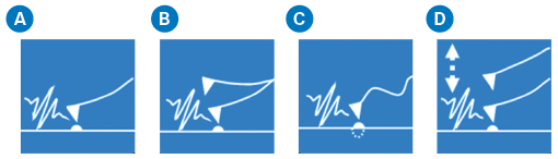
Figure 3. Major AFM-IR modes: (a) contact or Resonance-Enhanced mode, (b) Tapping AFM-IR mode, (c) Surface Sensitive mode, and (d) PeakForce Tapping AFM-IR mode. Image Credit: Bruker Nano Analytics
When it comes to choosing the right mode for AFM-IR measurement, the sample properties and the goal of the measurement should be taken into account. An outline of the AFM-IR modes, the laser source, sensitivity, spatial resolution, and likely applications are given in Table 1.
Table 1. Major AFM-IR modes implemented on the nanoIR/IconIR systems. Source: Bruker Nano Surfaces and Metrology
| Mode |
Laser
source |
Sensitivity |
Spatial
resolution (nm) |
Applications |
| Conventional |
Ekspla
OPO |
>50 nm |
>50 |
Polymeric and biological material with thickness >50 nm |
| Resonance-Enhanced |
Daylight QCL, M Squared Firefly; APE Carmina |
monolayer |
>20 |
Monolayer, single molecule |
Tapping
AFM-IR |
Daylight QCL, M Squared Firefly; APE Carmina |
monolayer |
<10 |
Loose particle, soft/sticky material |
| Surface Sensitive |
Daylight QCL,M Squared Firefly; APE Carmina |
monolayer |
<10 |
Multilayer, thin coating on bulk |
Conventional AFM-IR Mode
AFM-IR is usually performed in contact mode, with simple signal acquisition and low demands placed on the light source while still ensuring the primary advantage of correlation to transmission FTIR is maintained.
An analysis of the ringdown of the AFM cantilever oscillations is conducted after the sample absorbs IR radiation. This analysis is performed utilizing the fast Fourier transform (FFT) technique to rapidly determine amplitudes and frequencies. Resultingly, local absorption spectra can be produced by measuring the peak-to-peak intensity of the cantilever ringdown or the amplitude of the cantilever oscillation at a given frequency as a function of the source wavelength.
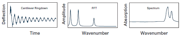
Figure 4. Diagrams of the cantilever ringdown, FFT, and spectrum for conventional AFM-IR operation. Image Credit: Bruker Nano Surfaces and Metrology
To capture detectable AFM-IR signal, the standard AFM-IR mode usually requires a sample thickness of more than 50 nm. An AFM-IR spectrum with a range of 1000 cm-1 takes in the region of 2-4 minutes to capture, while the laser wavelength is tuned incrementally.
Resonance-Enhanced AFM-IR Mode
Bruker’s patented Resonance-Enhanced mode was a key development and discovery which brought about significant improvements related to the sensitivity of AFM-IR via innovative developments made in Quantum Cascade Laser (QCL) technology.8
Typically, either a QCL or M Squared Firefly laser is applied as the mid-infrared laser source, and both lasers incorporate tunable pulse repetition rates. The AFM cantilever is put into contact mode as it interacts with the sample, while the laser pulse repetition rate is adjusted to match the contact resonance frequency of the cantilever.
Thermal expansion derives from how the sample absorbs infrared radiation, which facilitates uninterrupted excitation of the cantilever. This is unlike standard AFM-IR, which usually demonstrates decay in the ringdown. No specific contact resonance frequency needs to be selected for AFM-IR measurements.
Usually, when conducting AFM-IR spectroscopy, the second cantilever resonance frequency near 180 kHz is selected due to its exceptional signal-to-noise ratio. A Resonance-Enhanced AFM-IR spectrum is captured by plotting the amplitude of a selected cantilever resonance in the frequency domain as a function of the laser wavelength.
For AFM-IR imaging, it is possible to select a higher resonance frequency (>1 MHz) as it offers improved spatial resolution because of the reduced thermal diffusion length between two adjacent laser pulses.
The Resonance-Enhanced mode significantly improves AFM-IR sensitivity due to the AFM cantilever oscillation enhancement. The AFM-IR signal boost or gain from resonant excitation is Q/(2π), where Q represents the quality factor of the cantilever mode, expressed as the resonance amplitude over its full width at half maximum.
The signal amplification is usually 5 to 40 times with respect to the ringdown mode. This allows researchers to acquire AFM-IR measurements on thin samples, such as a self-assembled monolayer with a thickness as little as <1 nm on a silicon substrate.
The outstanding sensitivity of this mode has enabled measurements of infrared absorption spectra and chemical maps for a single protein molecule, with the results facilitating the true determination of the secondary structure of a single protein molecule that is in keeping with the structure of the bulk protein material.9
In contrast to the standard AFM-IR mode, the spatial resolution of Resonance-Enhanced mode demonstrates improvements and can reach levels as low as 20 nm for comparatively smooth samples.
The speed of Resonance-Enhanced AFM-IR spectroscopy has also been improved, as the laser wavelength is usually scanned in a fast sweep mode. A spectrum of 1000 cm-1 can be achieved in under 10 seconds.
To compensate for the mechanical difference between the sample’s various components, a phase-locked loop (PLL) is used to ensure correspondence between the laser pulse rate and ensures the contact resonance frequency of the cantilever is preserved on the sample.
Tapping AFM-IR Mode
Conducting AFM-IR measurements using a tapping technique marks another key breakthrough in the progression of the technology. Bruker has developed its own TappingMode™ to facilitate high-resolution topography measurements on rough, soft, or adhesive samples, which were once deemed impossible or presented researchers with significant obstacles when set in contact mode. The same can be said of Tapping AFM-IR.10,11
Tapping AFM-IR improves spatial resolution to below 10 nm, and in some instances, less than 5 nm. This development in spatial resolution permits the acquisition of practical infrared absorption images on samples with fine structures, including block copolymers and a variety of semiconductor samples with small domains.
Tapping AFM-IR can allow researchers to achieve high sensitivity when measuring thin monolayer samples. The AFM cantilever remains functional in TappingMode, in which a piezo actuator intermittently drives the probe oscillations at one of the cantilever resonance frequencies (f2 or f1) so that the tip contacts (i.e., ‘‘taps’’) the sample at interval rates. The Tapping AFM-IR signal is detected at an alternative resonance frequency (f1 or f2) and is relative to the absorption coefficient of the sample at the tip location.10
The set-up for the Tapping AFM-IR mode usually consists of a QCL or Firefly laser combined with various Tapping AFM-IR probes: the semi-soft TnIR-A probe runs at a frequency near 60 kHz at the first mode and a detection frequency near 380 kHz at the second mode.
The TnIR-D probe is stiffer and runs at a frequency near 1600 kHz at the second mode and is detected at the first mode near 250 kHz. Consequently, the higher signal-to-noise ratio of the TnIR-D probe makes it the default probe when running Tapping AFM-IR.
Surface Sensitive AFM-IR Mode
Surface Sensitive AFM-IR mode (SSM) is a Bruker proprietary mode that was developed fairly recently with the aim to isolate and only measure the top layer of a sample by restricting signal contributions from sub-surface material.12
In SSM, a soft AFM cantilever interacts with the sample in contact mode. Heterodyne detection is used for tuning the laser pulse repetition rate to correspond with the sum or difference of two contact resonance frequencies of the cantilever. This mode distinguishes itself from Tapping AFM-IR, which otherwise uses two tapping frequencies.
In SSM, drive of the cantilever runs at a high resonance frequency near 2 MHz and is detected at a lower resonance frequency around 180 kHz, with a comparatively high laser pulse repetition rate. This mix of experimental settings can improve surface sensitivity in contrast to both Resonance-Enhanced mode and Tapping AFM-IR mode.
For a traditional polymer sample, SSM has the ability to ensure signal contributions are limited to the top 10–30 nm of the sample.
PeakForce Tapping AFM-IR Mode
The PeakForce Tapping AFM-IR (PFIR) mode, developed by a Bruker collaborator Xiaoji Xu and their team, is a groundbreaking mode of the AFM-IR technique.13
PFIR makes use of Bruker’s patented PeakForce Tapping® mode, in which the AFM tip intermittently contacts the sample as the approach and retraction routines drive at several kilohertz.
PeakForce Tapping can be conducted at increased speeds in contrast to standard force curves as a result of the smart synchronized averaging and background subtraction mechanisms. This means the benefits of the off-resonant approach, i.e., delivering quantitative nanomechanical data, are preserved.
PFIR makes effective use of the contact time during each PeakForce Tapping cycle to transform the infrared absorption of the sample. This enables infrared spectroscopy and imaging capacities at sub-10 nm spatial resolution. Through close control of the interaction force between the AFM probe and the sample, PFIR can be used on rough and sticky samples.
Since PFIR is contingent on PeakForce Tapping, one major benefit is that it can map several key material properties simultaneously, including topographic, chemical, mechanical (e.g., adhesion, modulus), and electrical (e.g., surface potential).
AFM-IR in Liquid Mode
AFM-IR in liquid mode has been developed on the nanoIR system with the application of bottom-up illumination. The AFM-IR in Liquid mode has allowed researchers to resolve the secondary structures of protein samples in water. Results have demonstrated that there are comparable signal-to-noise and lateral resolutions taken from AFM-IR spectra and maps of samples in water to those in air.14
It was previously thought that capturing such measurements would be impossible due to water's strong absorption of mid-infrared. Further studies showed that Tapping AFM-IR works better than Resonance-Enhanced mode for samples in a fluid environment.
These developments reveal that AFM-IR has great analytical potential and can be applied to various air-sensitive samples. As alternatives to immersion in a liquid phase, it is also possible to prepare selected samples as nanodroplets on a substrate with a nanospray, or sealed in a hydrated environment with a thin hydrogel coating.15,16
Samples can, therefore, be measured using the standard top-down illumination method and are more likely to preserve the native structures in liquid.
Experimental Accessories and Laser Sources
For insights on experimental accessories and laser sources, see Bruker’s full application note, ‘A Comprehensive Guide to Photothermal AFM-IR Spectroscopy’.
Conclusion
Photothermal AFM-IR is a renowned technique and is a good match for comparison with transmission FTIR data due to a good understanding of its underlying physics. This allows researchers to gain key insights from bulk spectroscopy that can be directly applied at the nanoscale.
When working at the nanoscale, several key factors should be taken into account when conducting measurements, processing, and characterization of AFM-IR spectra, which have been detailed in this article.
An understanding of these factors and AFM-IR spectroscopy at large allows researchers to perform sub-diffraction measurements that can be used on polymer, biological, semiconductor, and inorganic samples to generate a diverse range of characterization pathways.
References
- A C Jones, and M B Raschke, Nano Letters 12, 1475 (2012). DOI: 10.1021/nl204201g
- D Kurouski, Vibrational Spectroscopy 91, 3 (2017). DOI: 10.1016/j.vibspec.2016.06.004
- A Dazzi, R Prazeres, F Glotin, and J M Ortega, OPTICS LETTERS 30, 2388 (2005). DOI: 10.1364/ol.30.002388
- A Dazzi, F Glotin, and R Carminati, Journal of Applied Physics 107, 124519 (2010). DOI: 10.1063/1.3429214
- J J Schwartz, D S Jakob, and A Centrone, Chemical Society Reviews 51, 5248 (2022). DOI: 10.1039/D2CS00095D
- C Marcott, M Lo, K Kjoller, C Prater, and I Noda, Applied Spectroscopy 65, 1145 (2011). DOI: 10.1366/11-06341
- A Dazzi, and C B Prater, Chemical Reviews 117, 5146 (2017). DOI: 10.1021/acs.chemrev.6b00448
- F Lu, M Jin, and M A Belkin, Nature Photonics 8, 307 (2014). DOI: 10.1038/nphoton.2013.373
- F S Ruggeri, B Mannini, R Schmid, M Vendruscolo, and T P J Knowles, Nature Communications 11, 2945 (2020). DOI: 10.1038/s41467-020-16728-1
- J Mathurin, E Pancani, A Deniset-Besseau, K Kjoller, C B Prater, R Gref, and A Dazzi, Analyst 143, 5940 (2018). DOI: 10.1039/C8AN01239C
- F Tarpoudi Baheri, T M Schutzius, D Poulikakos, and L D Poulikakos, Journal of Microscopy 00, 1 (2020). DOI: 10.1111/jmi.12890
- International Patent WO2020049053; United States Patent US 11,215,637 B2
- L Wang, H Wang, M Wagner, Y Yan, D S Jakob, X G Xu, Science Advance 3, e1700255 (2017). DOI: 10.1126/sciadv.1700255
- G Ramer, F S Ruggeri, A Levin, T P J Knowles, and A Centrone, ACS Nano 12, 6612 (2018). DOI: 10.1021/acsnano.8b01425
- A Miller, S Chia, Z Toprakcioglu, T Hakala, R Schmid, Y Feng, T Kartanas, A Kamada, M Vendruscolo, F S Ruggeri, and T P J Knowles, Science Advance 9, eabq3151 (2023). DOI: 10.1126/sciadv.abq3151
- A P Fellows, M T L Casford, and P B Davies, Biophysical Journal 119, 1474 (2020). DOI: 10.1016/j.bpj.2020.09.007

This information has been sourced, reviewed and adapted from materials provided by Bruker Nano Analytics.
For more information on this source, please visit Bruker Nano Surfaces and Metrology.