Sponsored by Avantes BVReviewed by Maria OsipovaAug 15 2024
Nonthermal and thermal plasmas are utilized in various engineering, industrial, medical, and research applications. The composition of the plasma is a crucial parameter for any plasma process. Optical emission spectroscopy allows for accurate, almost real-time monitoring of plasma in chambers and on plasma-contacting substrates, which facilitates inline process monitoring and optimization.
Introduction
“Plasma” refers to a gas with a significant proportion of ionized molecules, which produce various excited ions, atoms, and molecules.
Electrons liberated from ions and atoms are highly energetic and can travel freely throughout the plasma. These high-energy electrons can run into neutral atoms and molecules, causing a transfer of a portion of their energy. As the neutral molecules and atoms revert to their ground state, they emit light photons. The color of that light depends on the photon energy, which depends on the energy difference between the excited and ground states of the neutral atoms and molecules.
When unbound charged particles are present, they affect the bulk electromagnetic properties of plasmas; they possess electrical conductivity and can be confined and shaped by magnetic fields.
Ionization means that plasmas have the potential to be highly reactive, while raised temperatures (and thus high particle velocities) in thermal plasmas are enough to cause substrate ablation.
Plasmas can be produced at various temperatures and pressures. Tuning these parameters and altering the chemical species found in plasma can dramatically affect plasma behavior and produce plasmas suitable for various applications. Precise control of these parameters is essential for maintaining reliable, stable, and reproducible processes.
Key Plasma Parameters
Plasmas can be widely characterized in terms of temperature, pressure, and the chemical species present in them in industry and research.
Similar to gases and other substances, plasma temperature can be measured in kelvin and relates directly to the thermal kinetic energy per particle. Of important note, however, is that because of the difference in mass between electrons and ions, the effective temperature of the ions in plasma may differ greatly from that of the electrons.
In electromagnetically confined plasmas, energy is usually transferred more efficiently to electrons than ions, raising the electron temperature. Energy transfer from electrons to ions and from ions to the environment decides the ion temperature.
In nonthermal or “cold” plasmas, the ions move heat quickly to their surroundings before reaching high temperatures. This means that most of the thermal energy in the plasma is stored inside the electrons rather than the ions, which results in a generally relatively low temperature. Nonthermal plasmas are typically touch-safe and able to be used in medical applications and in collaboration with heat-sensitive materials.1
By contrast, thermal plasmas have an ion temperature near the electron temperature. The particle energies in thermal plasmas are usually enough to ablate surfaces, allowing them a range of applications in polishing, etching, and surface-texturing processes. Thermal plasmas have even more applications in physical and chemical vapor deposition processes that allow precise coating deposition.2,3
Several plasma applications are performed under vacuum conditions because a decrease in pressure lowers the rate of electron-ion recombination and collisions with other molecules, increasing plasma particles' mean free path. However, recent developments in plasma technology have allowed for an increase in plasma applications at atmospheric pressure.
The chemical species in the plasma mostly depend on the gas used in the process. However, the pressure and temperature also greatly alter the composition. As plasma color directly relates to composition, the variety of chemical species will also affect the color.
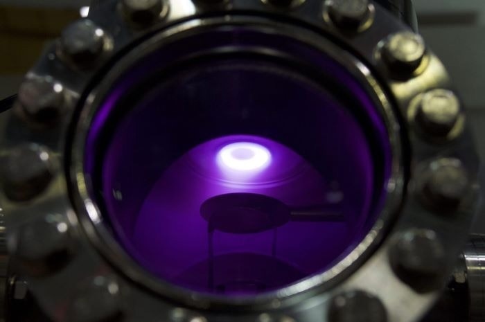
Plasma Vacuum Chamber. Image Credit: Avantes BV
Optical Spectroscopy for Plasma Analysis
Plasma composition is a crucial parameter in all types of plasma applications. In engineering, industry, and medicine, precision process control and reproducibility are only ensured by in-depth characterization of molecular species in the plasma and on surfaces.
Optical emission spectroscopy is a general term for methods that measure optical absorption/emission spectra, i.e., the light emitted when a sample is in the excited state. It is a significant technique in plasma analysis because it allows accurate non-contact characterization of the plasma color and the species present.
Optical spectroscopy works well with harsh thermal plasma environments and applications sensitive to contamination. It offers close to real-time feedback, allowing inline process monitoring and resulting in fast, responsive process optimization in various plasma applications.
Vacuum Plasma Applications
One of the more common vacuum applications in plasma is the plasma etch process in semiconductor manufacturing.4 This advanced application involves the precise and controlled removal of surface material to create patterns on silicon wafers.
Plasma etching in semiconductor devices demands highly precise monitoring throughout the reaction progress, otherwise known as endpoint detection, and is also highly prone to contamination. These considerations mean that plasma etching demands great accuracy in plasma analysis. Optical emission spectroscopy—commonly across the near-infrared to near-ultraviolet regions of the spectrum—offers the required stability, speed, and resolution for inline process control in plasma etch applications.
Vacuum plasma systems are also utilized in depositing coatings and thin films through a variety of plasma-driven chemical vapor deposition (CVD) and physical vapor deposition (PVD) processes, particularly in plasma-enhanced chemical vapor deposition (PECVD), sputtering, and ion beam deposition.
These processes typically involve harsh operating conditions caused by the high plasma energies and extremely reactive plasma species. Optical emission spectroscopy is key in plasma analysis for these applications as it offers a non-contact solution: optical fibers allow accurate standoff measurements of the process environment.
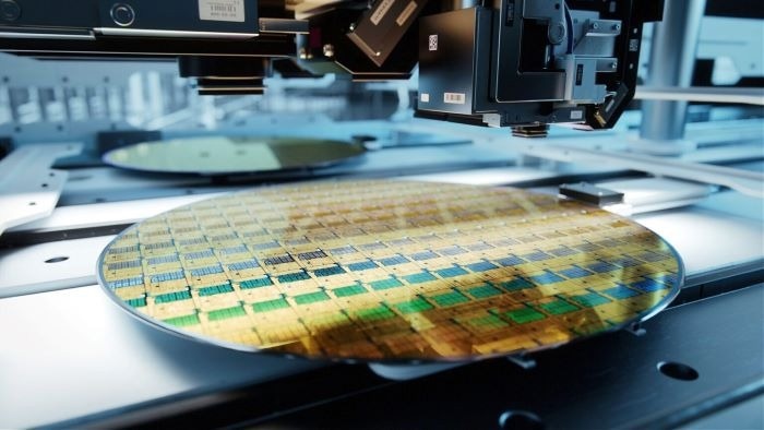
Silicon wafer inline process control. Image Credit: Avantes BV
Atmospheric Pressure Plasma Applications
Several applications have been reported for nonthermal atmospheric pressure plasmas in medical applications as they effectively sterilize tissues and tools. In addition, they can be tuned for other purposes, including cell detachment, genetic transfection, and wound healing.1,5,6
Fiber optic spectrometers are of particular value in medical plasma applications, where disposable fiber optic interfaces provide low-cost disposable testing compatible with hygienic in vivo applications.7
Atmospheric plasmas are widely used for surface finishing and modification. Electrolytic plasma polishing (EPP) concerns producing atmospheric pressure plasmas in electrolytic baths to finish metal surfaces, whereas the reactive atom plasma (RAP) process has proven effective in figuring optical components.8,9 In these applications, optical emission spectroscopy offers a cost-effective and rapid plasma analysis solution well suited for inline analysis and process control.
Close to real-time feedback means that optical emission spectroscopy has a crucial part in plasma analysis in a large array of other atmospheric pressure plasma applications:
- Inductively coupled plasma mass spectrometry (ICP-OES) is a commonly used method for elemental analysis. In this method, atmospheric pressure plasma ionizes a sample before spectroscopic analysis.
- Plasma aerodynamics is a fast-growing field that is looking to utilize plasmas to control aerodynamic processes. For instance, controlling laminar to turbulent transitions, suppressing local heating, and reducing drag.10,11
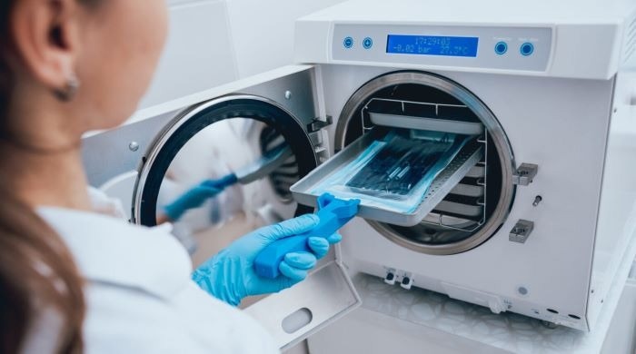
Sterilizing medical tools. Image Credit: Avantes BV
Avantes Optical Spectroscopy Systems for Plasma Analysis
Optical emission spectroscopy is ideal for non-invasive measurement techniques for plasma diagnostics in hostile plasma environments while guarding against contamination.
However, plasmas are commonly characterized by many closely spaced emission peaks. Creating separation in these peaks demands an optical spectroscopy system with high spectral resolution.
Multichannel spectrometer systems from Avantes offer especially high spectral resolution for advanced plasma applications, which can allow the characterization of vibrational and rotational distribution functions of electronically excited molecules.
CCD sensors have long dominated spectroscopy applications. However, newer devices like the Avantes-developed AvaSpec-ULS4096CL-EVO use CMOS sensors to achieve quicker and more accurate performance.
The AvaSpec-ULS4096CL-EVO offers integration times down to 9 μs and up to 0.05 nm resolution within the range from 200 nm to 400 nm using a 3600-groove density grating, so it is suitable for even the most stringent plasma analysis applications.
 Download the article to learn more
References and Further Reading
- Fridman, G.et al. Applied Plasma Medicine. Plasma Processes and Polymers 5, 503–533 (2008).
- Martinu, L. & Poitras, D. Plasma deposition of optical films and coatings: A review. Journal of Vacuum Science & Technology A: Vacuum, Surfaces, and Films 18, 2619–2645 (2000).
- Eskildsen, S. S., Mathiasen, C. & Foss, M. Plasma CVD: process capabilities and economic aspects.Surface and Coatings Technology 116–119, 18–24 (1999).
- Darnon, M. Plasma Etching in Microelectronics. In Plasma Etching Processes for CMOS Devices Realization 23–58 (Elsevier, 2017). doi:10.1016/B978-1-78548-096-6.50002-X.
- Bekeschus, S., von Woedtke, T., Emmert, S. & Schmidt, A. Medical gas plasma-stimulated wound healing: Evidence and mechanisms. Redox Biol 46, 102116 (2021).
- Scholtz, V., Pazlarova, J., Souskova, H., Khun, J. & Julak, J. Nonthermal plasma — A tool for decontamination and disinfection. Biotechnology Advances 33, 1108–1119 (2015).
- Medical/Biomedical. Avantes https://www.avantes.com/applications/markets/biomedical-medical/.
- Huang, Y. et al. Principle, process, and application of metal plasma electrolytic polishing: a review. Int J Adv Manuf Technol 114, 1893–1912 (2021).
- Jourdain, R., Castelli, M., Morantz, P. & Shore, P. Plasma surface figuring of large optical components. 8430, 843011 (2012).
- Jonathan, P., Thomas, M. & Sergey, L. Plasma Aerodynamics : Current Status and Future Directions. AerospaceLab Journal Issue 10, 6 pages (2015).
- Mohamed, A.-A. H., Fadhlalmawla, S. A. & Almarashi, J. Q. M. The shift in the laminar-to-turbulent transition flow mode in atmospheric pressure plasma jet. Plasma Processes and Polymers n/a, e2200145.

About Avantes
With over 30 years of expertise, Avantes is the leading innovator in developing fiber-optic spectroscopy instruments and systems. Our dedication to excellence and customer satisfaction has made us a trusted partner in the nanotechnology sector, supporting a wide range of applications from material characterization to nanoscale research.
Our Expertise in Nanotechnology
At Avantes, we pride ourselves on our collaborative approach, working closely with nanotechnology professionals to develop spectrometer configurations tailored to their specific needs. Our advanced spectrometers, light sources, and fiber-optic sampling accessories enable precise measurements in ultra-violet, visible, and near-infrared wavelengths, essential for applications such as nanoparticle analysis, thin-film measurements, and semiconductor research.
Global Reach and Proven Performance
With over 53,000 systems installed worldwide, our solutions are integral to the nanotechnology community. We provide state-of-the-art technology for spectroscopy and material characterization, ensuring our customers achieve the highest levels of accuracy and reliability in their measurements.
Products and Services for Nanotechnology
We offer a comprehensive range of products designed to meet the diverse needs of the nanotechnology field:
- Spectrometers: High-resolution, miniature fiber optic spectrometers with options for PDA, CMOS, CCD, back-thinned CCD, and InGaAs detectors, ideal for nanoscale measurements.
- Optical Benches: Featuring focal lengths of 45, 50, or 75 mm, including our revolutionary ultra-low straylight optimized optical bench (ULS) and high-sensitivity optical bench, perfect for demanding nanotechnology research.
- Light Sources: Including tungsten-halogen, deuterium, LED, and xenon calibration sources to support a wide range of spectroscopy techniques in nanotechnology.
- Fiber Optics: Offering a comprehensive selection of fiber optics for efficient light transmission and sampling in various spectroscopic applications.
- Accessories: Comprehensive selection of fibers, sampling accessories, and custom software to enhance your spectroscopic experiments.
Supported Techniques for Nanotechnology
Our instruments support a variety of essential measurement techniques:
- UV-VIS/NIR spectroscopy for analyzing nanoscale materials and chemical compositions
- Absorbance, transmittance, and reflectance for evaluating material properties
- Fluorescence spectroscopy for studying nanomaterials and their interactions
- Raman spectroscopy for detailed molecular and structural characterization
- Laser-induced breakdown spectroscopy (LIBS) for elemental analysis at the nanoscale
- Differential optical absorption spectroscopy (DOAS) for precise measurements
- Irradiance and radiometry for accurate light measurements
Commitment to OEM Partnerships in Nanotechnology
For OEM customers in the nanotechnology sector, we adopt a partnership approach to tailor our solutions and manufacturing processes to the specific needs of end-use applications. Our sales engineers engage in a thorough discovery process to ensure our solutions align perfectly with your requirements. Our team collaborates closely with OEM partners to ensure seamless integration and optimal performance, leveraging our automated manufacturing process, 'AvaMation,' for unmatched reproducibility and scalable production.
Industries We Serve in Nanotechnology
Our versatile solutions cater to various sectors within nanotechnology, including:
- Nanomaterials research
- Semiconductor industry
- Thin-film measurement
- Photonics
- Surface science
- Environmental nanotechnology
Our Mission
At Avantes, we are dedicated to continuously driving innovation in spectroscopy, empowering nanotechnology professionals with the most reliable and advanced solutions. We are committed to exceeding expectations and providing the support needed to achieve groundbreaking discoveries and advancements in the nanotechnology field.
Visit our website to learn more about how our spectroscopy solutions can support your nanotechnology research and applications.
For more information on this source, please visit Avantes BV.
This information has been sourced, reviewed and adapted from materials provided by Avantes BV.