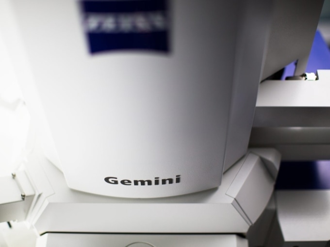
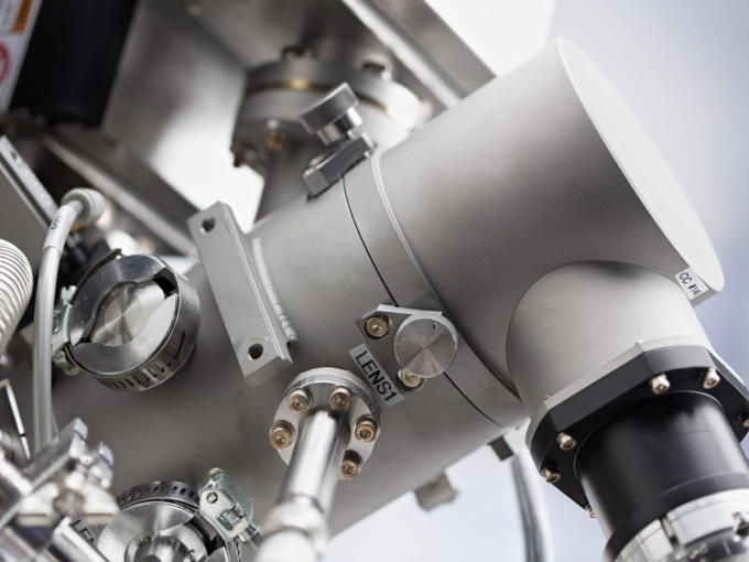
The ZEISS Crossbeam doubles up as a 3D nano-workstation. The imaging and analytical performance of a field emission scanning electron microscope (FE-SEM) can be combined with the processing ability of a focused ion beam (FIB). During imaging, milling, or when performing 3D analytics, the Crossbeam accelerates the FIB applications. The new EDS module enables conducting 3D analytics. While variable pressure capabilities can be exploited with the ZEISS Crossbeam 340, the Crossbeam 550 can be used for the most demanding characterizations. The large chamber now offers more options.
Advantages in FIB-SEM
Maximize Your SEM Insights

The FIB-SEM offers 30% better SEM resolution at low voltage.
The ZEISS Crossbeam delivers excellent SEM performance during 3D tomography or 2D surface sensitive images. The Gemini optics has a resolution down to 1.4 nm at 1 kV acceleration voltage which allows obtaining high-quality images from any sample by simply applying a voltage to the sample with Tandem decel. Various types of detectors allow comprehensive characterization of samples, and the unique Inlens EsB detector enables pure materials contrast effect. Non-conductive specimens can be studied without any disturbance from charging artifacts.
Increase Your FIB Sample Throughput

The intelligent FIB milling strategies enable 40% faster material removal.
The highest ion beam current, provided for any gallium FIB-SEM, is available for use. A significant amount of time can be saved with excellent FIB profiles using up to 100 nA current without affecting the ultimate FIB resolution. The precision and speed of intelligent FIB scanning strategies for material removal can benefit users. Batches of samples, like TEM lamellae, cross-sections, or any user-defined pattern can be automatically prepared.
Experience Best 3D Resolution in Your FIB-SEM Analysis

The integrated 3D EDS analysis provides a number of benefits.
The capacity of Crossbeam can be expanded with ZEISS Atlas 5, the market-leading package for fast, precise tomography. During tomography, the EDS analysis can be conducted using the integrated 3D Analytics module of ZEISS Atlas 5. The ZEISS Crossbeam features the Gemini optics and a FIB customized for speed and precision. Users can benefit from the best 3D resolution and leading isotropic voxel size in FIB-SEM tomography. Using the Inlens EsB detector, users can probe less than 3 nm in depth and create surface-sensitive, material-contrast images.
ZEISS Crossbeam: FIB-SEM for High Throughput 3D Analysis and Sample Preparation
High resolution at FIB-SEM coincidence
The point where the stage and SEM- and FIB beam join for FIB patterning, deposition or milling: Alumina nanospheres imaged at 1 kV with Tandem decel.
Cross-sectioning with 100 nA
The FIB column of the ZEISS Crossbeam Family is uniquely equipped with a beam current of 100 nA. This trench is milled in silicon, dimensions 100 × 30 × 25 μm³, milling time 10 minutes using 100 nA FIB current. Note the precision of the structure.
Comparison of milling strategies in silicon:
Material removal with convential milling (left) takes 10 min 54 sec whereas with Fastmill the same amount of material is removed in 7 min 21 sec (right). With Fastmill, a newly-introduced scanning strategy, milling speed is enhanced by optimally exploiting the angle-dependent sputtering effect. Fastmill enables up to 40% faster milling than regular line milling.
Precise sample preparation in a dense matrix
TEM-Lamella of a silver/nickel/copper-layered system ready for lift out, fabricated with automatic sample preparation.
Preparation of batches
Array of TEM lamellae fabricated with automated preparation.
EDS analysis at very high resolution with STEM
Chromium carbides at the grain boundary of thermally-affected X2CrNi18-10 steel: STEM BF (left), EDS chromium map (right).
Nanofluidic channels, master stamp
Nanofluidic channels, meander-shaped channels
Nanofluidic channels, funnel-shaped inlets and outlets