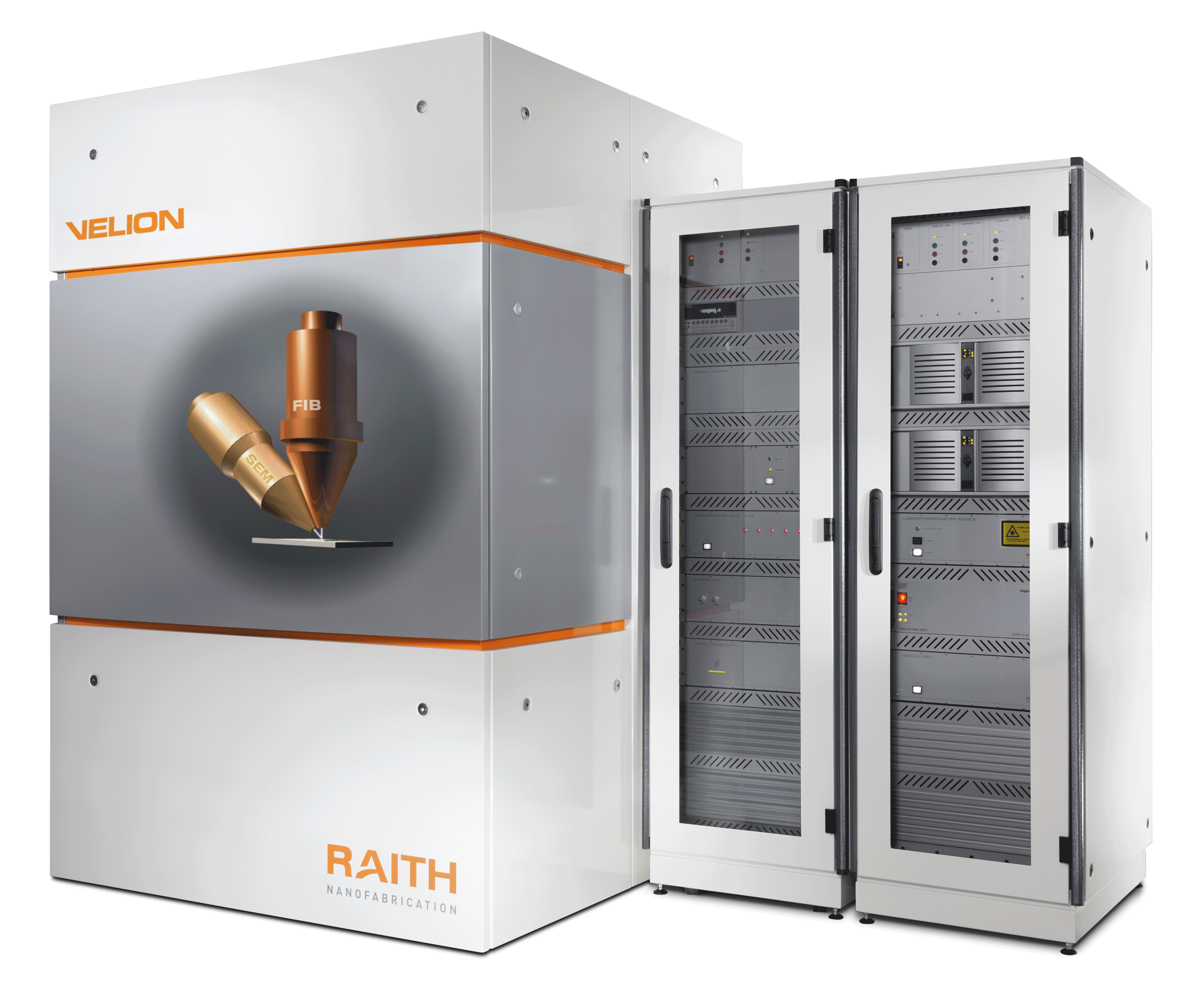
Focused Ion Beam (FIB) technology provides very versatile capabilities for manufacturing a number of materials. Therefore VELION is a FIB-SEM system dedicated to nanofabrication where FIB is the main techniques. Thus the instrument is highly optimized for fabricating high resolution, three dimensional nanostructures like lenses, plasmonic devices, localized implantation, metamaterials, nanofluidics, and more.
With the support of a tailored FE-SEM column and Raith’s high-precision laser interferometer stage, VELION allows for multipurpose use in four different operation modes. FIB nanofabrication, sample preparation, e-beam lithography and process control are now possible with a single tool.
The unique architecture makes VELION a FIB prioritized system, designed to meet the most demanding nanofabrication requirements. It provides a range of direct FIB processing methods with the unparalleled stability, reproducibility, automation, and high resolution of a lithography instrument.
Image credit: Raith
FIB methods can make nanofabrication more efficient by using direct patterning (milling, etching, deposition) or hard masking, and permit new processes based upon maskless ion implantation or surface functionalization.
VELION is the result of developments to answer to the fast- growing interest in ion beam based nanofabrication in a range of areas of R&D. Its unique nanoFIB Three ion column delivers superior placement accuracy, high resolution, long-term stability and record low beam tails. The tailored FE-SEM column as well as further options such as gas injection systems, nanoprobers, and EDX support the FIB processes and majorly expand the application range.
VELION Product Details
Main Uses
- Direct and 3D FIB techniques
- Gas-free FIB nanofabrication
- Nanoengineering platform
- Sample preparation
- SEM inspection and lithography
Unique writing mode
Stage
- 4” full travel
- Large Z travel
- Rotation and tilt sample holder
- Other tilt setups
Column technology
- nanoFIB Three
- IONselect
- Ion column 35 kV Ga (Au, Si, Ge)
- FE-SEM column 30 kV
Focused Ion Beam Benefits
- True 3D direct patterning, also on topographic samples
- Simplified processes and process development for fastest time to results
- Versatile FIB methods for challenging or new materials
Advanced FIB Nanofabrication
- Guaranteed sub-10 nm FIB nanofabrication and outstanding beam spot characteristics
- Multiple ion species beyond gallium (IONselect technology)
- Lithography-class stability and accuracy over extended periods of time and areas
- Laser interferometer stage for maximum precision and true field stitching or continuous patterning
SEM and more
- SEM inspection for in-situ process control
- Live-imaging during TEM sample preparation
- Gas-assisted processes, manipulation, and probing
Configurable Setups for Extended Versatility
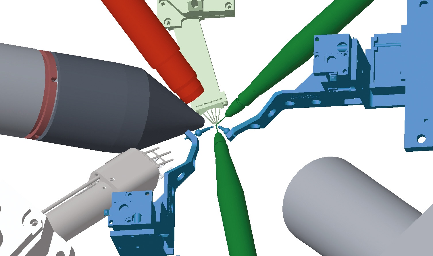
With various universal ports on the vacuum chamber, VELION supports a configurable setup that can be upgraded in the future. As well as other features, the FIB-SEM system can be fitted with a range of multiline and mono-line gas injection systems. Inclusion of multiple GISs from opposite directions allows for gas-induced processes such as wiring of nano-objects and X-section analysis. Gas-assisted etching offers better selectivity, improved removal rates, and less redeposition.
A new added feature is a nanoprofilometer as an add-on option, which allows both 3D process control and lateral secondary electron imaging information. The 3D surface imaging solution nanoSense helps to qualify etching, deposition, and milling processes in situ within minutes. Additional options include various optical cameras, sample auto height sensing, plasma sample cleaner, EDX, and more.
CAD view of a VELION setup including SEM, SE and EDX detector, 5-channel and two single line GIS, optical macroscope as well as two nano manipulators. Image credit: Raith
IONselect Technology - FIB Nanofabrication Beyond Gallium
The nanoFIB Three technology is used for continuous delivery of silicon, gold, or other ions with nanometer beam diameters. The flow-enhanced alloy ion source and low-aberration ion optics allow easy switching between numerous ion species from a single source, while maintaining the high resolution and stability of the nanoFIB Three column.
IONselect provides a range of species, from doubly charged light ions to heavy ions and clusters - all with superior handling and enabling different yet-to-be-explored nanofabrication methods. Processing that involves specific functionalization, low contamination, higher resolution, or surface sensitive milling will open doors for new breakthroughs in next-generation research.
VELION - FIB-SEM where FIB truly comes first

 Download the brochure here
VELION: FIB-SEM Where FIB Truly Comes First

1-mm long fluidic channel fabricated by milling with stitching

The 3-dimensional shape of a special antireflective grating is revealed by X-section analysis (Image Credits: Bilkent University)

SEM control of a test array on a membrane

EBL test pattern for line width and dose

Direct FIB milling for a 3-dimensional absorber structure (Image Credits: Zhejiang University)

Part of a wave guide and photonic crystal pattern in resist

FIB cutting sub-10 nm features in challenging materials like polycrystalline gold (Image Credits: University of Stuttgart)

High-resolution imaging of plasmonic features created by FIB milling (Image Credits: University of Stuttgart)

TEM lamella preparation by in-situ lift out (Image Credits: NMI Reutlingen)

Write field stitching allows for direct milling of long waveguides with offsets on the 10 nm scale only (Image credits: Peking University)