Oct 22 2009
Jun Akedo and Akito Endo, the Advanced Manufacturing Research Institute of the National Institute of Advanced Industrial Science and Technology (AIST) have succeeded in developing a high-speed printing technology that involves laser irradiation during ink-jet printing.
 Fine wire with high aspect ratio (thickness/width)
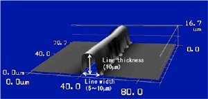
The line width is scaled down while the line thickness is increased. Fine conductor patterns less than 10 µm in line width are successfully printed at a speed of 10 mm/sec without reprinting and with an aspect ratio (thickness/width) higher than unity. This is what has been difficult to be realized using existing industrial ink-jet technologies. It is confirmed that our newly invented laser-assisted ink-jet printing (LIJ) technology can print thin wires with a high aspect ratio by using ultrafine metal particle ink on various types of substrates regardless of substrate surface conditions such as steps of up to several hundred µm, material and roughness.
The wire (10 µm in line width) produced by the LIJ technology has a resistance per unit length of as low as 6 O/cm due to the high aspect ratio. This is a great improvement over the existing industrial ink-jet printing technologies using ultrafine metal particle ink where the interconnection resistance would typically be 70 O/cm for a line width of 10 µm.
Using the developed technology, low-resistance wires can be printed at high speed for the interposers between chips and a main board, wiring on flexible resin members, step connections between metal parts, and high-density wiring on curved surfaces. The technology will greatly improve the efficiency of development and production of microelectronic devices.