Today, Carl Zeiss introduces EVO® HD, its latest innovation in the conventional Scanning Electron Microscopy (C-SEM) market segment. Delivering much higher resolution at low acceleration voltages compared to present conventional SEM, the EVO® HD introduces High Definition to electron microscopy.
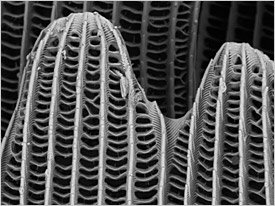 Scale of butterfly wing (Pieris Brassicae) taken on the new EVO®HD electron microscope at 5kV acceleration voltage. The combination of the groundbreaking high source brightness of the EVO® HD and the enhanced low-kV sensitivity of the detector allows for more insight into such non-conductive biological nano-structures. Nano-textures associated with biological structures have attracted considerable attention not just in Zoology, but also in Material Science, bio-mimicry and nano-engineering.
The technological basis for this achievement is the new EVO® HD source which features a higher source brightness. This brightness results in an improvement in resolution at low-kV relative to conventional tungsten SEMs. The improved source properties also aid analytical applications with a 30% increase in resolution at 30kV and 1nA.
“We are convinced that this is the most significant innovation in the market for conventional SEM in the last decade. Numerous applications in both life sciences and materials analysis will benefit from the increased performance”, explains Allister Mc Bride from Carl Zeiss Nano Technology Systems division at Cambridge.