Scientists at the U.S. Department of Energy's (DOE) Brookhaven National Laboratory and Los Alamos National Laboratory have fabricated transparent thin films capable of absorbing light and generating electric charge over a relatively large area.
The material, described in the journal Chemistry of Materials, could be used to develop transparent solar panels or even windows that absorb solar energy to generate electricity.
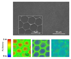
 Scanning electron microscopy image and zoom of conjugated polymer (PPV) honeycomb. Bottom (left-to-right): Confocal fluorescence lifetime images of conjugated honeycomb, of polymer/fullerene honeycomb double layer and of polymer/fullerene honeycomb blend.
The material consists of a semiconducting polymer doped with carbon-rich fullerenes. Under carefully controlled conditions, the material self-assembles to form a reproducible pattern of micron-size hexagon-shaped cells over a relatively large area (up to several millimeters).
"Though such honeycomb-patterned thin films have previously been made using conventional polymers like polystyrene, this is the first report of such a material that blends semiconductors and fullerenes to absorb light and efficiently generate charge and charge separation," said lead scientist Mircea Cotlet, a physical chemist at Brookhaven's Center for Functional Nanomaterials.
Furthermore, the material remains largely transparent because the polymer chains pack densely only at the edges of the hexagons, while remaining loosely packed and spread very thin across the centers. "The densely packed edges strongly absorb light and may also facilitate conducting electricity," Cotlet explained, "while the centers do not absorb much light and are relatively transparent."
"Combining these traits and achieving large-scale patterning could enable a wide range of practical applications, such as energy-generating solar windows, transparent solar panels, and new kinds of optical displays," said co-author Zhihua Xu, a materials scientist at the CFN.
"Imagine a house with windows made of this kind of material, which, combined with a solar roof, would cut its electricity costs significantly. This is pretty exciting," Cotlet said.
The scientists fabricated the honeycomb thin films by creating a flow of micrometer-size water droplets across a thin layer of the polymer/fullerene blend solution. These water droplets self-assembled into large arrays within the polymer solution. As the solvent completely evaporates, the polymer forms a hexagonal honeycomb pattern over a large area.
"This is a cost-effective method, with potential to be scaled up from the laboratory to industrial-scale production," Xu said.
The scientists verified the uniformity of the honeycomb structure with various scanning probe and electron microscopy techniques, and tested the optical properties and charge generation at various parts of the honeycomb structure (edges, centers, and nodes where individual cells connect) using time-resolved confocal fluorescence microscopy.
The scientists also found that the degree of polymer packing was determined by the rate of solvent evaporation, which in turn determines the rate of charge transport through the material.
"The slower the solvent evaporates, the more tightly packed the polymer, and the better the charge transport," Cotlet said.
"Our work provides a deeper understanding of the optical properties of the honeycomb structure. The next step will be to use these honeycomb thin films to fabricate transparent and flexible organic solar cells and other devices," he said.
Source: http://www.bnl.gov/