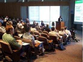
Following the success of last year's seminar and workshop programme, Oxford Instruments Plasma Technology will again hold several similar events this year in conjunction with key research institutes & universities globally. Speakers will come from the host universities and from a number of other institutes and industry, in addition to process and applications experts from Oxford Instruments Plasma Technology, providing their in-depth knowledge of the chosen topic.
 Oxford Instruments co-hosts a number of successful seminars annually
March 11-12th 2011 - Nanoelectronics: Growth, deposition, etching
Hosted by the Institute of Semiconductors Chinese Academy of Sciences (IOS) & Oxford Instruments in Beijing
June 30th 2011 - Knowledge creation partnership - from funding to results
Workshop hosted by the University of Southampton & Oxford Instruments at the University of Southampton
July 14-15th 2011 - New Frontiers in Plasma Nano patterning
Hosted by the Molecular Foundry, Lawrence Berkeley National Laboratory, CA, USA
The company also plans to hold a Seminar/Workshop in France, date to be confirmed.
Programmes are available, and for more information about each seminar and/or to register for a place email: [email protected]
Oxford Instruments' etch, deposition and growth systems provide process solutions for the micro- and nanometre engineering of materials for semiconductor, optoelectronics, MEMS & microfluidics, high quality optical coating and many other applications in micro- and nanotechnology.