Feb 24 2011
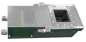
USHIO America, Inc. (Headquarters: Cypress, California; President and Chief Executive Officer: Kenji Hamashima), a leading provider of specialty and general- illumination lighting solutions as a wholly owned subsidiary of USHIO Inc. (TOKYO:6925)(Headquarters: Tokyo, Japan; President and CEO: Shiro Sugata), today announced that the company plans to start marketing the nano-imprint VUV (Vacuum Ultra Violet) ashing system "CHIPs (Compact HiPower System)" in the US on March 1, 2011.
Incorporated into the nano-imprint lithography (NIL) equipment to be used for fabricating circuit patterns of a variety of devices including LEDs, MEMS, functional films, and biochips, the CHIPs allows non-contact and damage-free cleaning, surface improvement, and ashing of templates and workpieces.
 USHIO Develops and Begins Marketing Nano-Imprint VUV Ashing System "CHIPs."
NIL is a lithography technology that transfers a circuit pattern by directly imprinting a template (or mold) with the circuit pattern on a workpiece (a resist-coated silicon, sapphire, or film substrate). It has the advantage of being a low-cost process, allowing large-area pattern transfer, and being suitable for mass-production. NIL already has been put into practical use for fabricating circuit patterns with a line width at a micro-meter (µm) level. NIL has evolved with further research and development efforts to establish a finer-pattern process technology at a nano-meter (nm) level.
Today, the NIL process faces the following challenges caused by putting a workpiece into contact with a template, and they are becoming obstacles for fabricating finer patterns as well as enhancing productivity:
Challenges for NIL:
- Contamination of templates with resist residue
- Increase in resist fill time and fill failures
- Deterioration of release property between a template and a workpiece
Problems in Conventional Solutions
Wet- or dry-cleaning equipment needs to be separately installed to clean the templates used for a certain number of process cycles by removing them from the NIL equipment. This causes downtime, thus lowering the productivity. Also, the wet-cleaning equipment has some disadvantages: it has an insufficient cleaning capability, causes a risk of generating chemical residue, and requires additional processes (such as drying and waste disposal). The dry-cleaning equipment using plasma, meanwhile, has disadvantages in that it causes damage to a workpiece and requires additional components (such as a vacuum chamber).
Solutions by CHIPs
In order to meet these challenges, USHIO successfully developed its new nano-imprint VUV ashing system "CHIPs" by applying and optimizing its lighting-edge technologies to NIL to achieve non-contact and damage-free high cleaning power using VUV light. In addition, the CHIPs can be incorporated into the NIL equipment to allow a reduction of the downtime of the NIL equipment as well as automation of the NIL process — thus enhancing the productivity and yield and thereby lowering the CoO of the NIL process.
USHIO will exhibit and participate in the "SPIE Advanced Lithography 2011" conference, to be held on February 27 (Sun.) through March 3 (Thu.), 2011, at the San Jose Convention Center and San Jose Marriot (Headquarters Hotel) in San Jose, California, USA (Booth No. 428).
USHIO will strive to work on providing lighting-edge solutions for a variety of challenges in processing of finer patterns of various devices.
Source: http://www.ushio.co.jp/en/