WaferSense Auto Gapping System to Help 300 mm fab Boost Accessibility of PECVD Tool
The Auto Gapping System from CyberOptics Semiconductors is a new edition of its legacy gapping technology that needed 10 hours to determine how far the chamber’s gas showerhead was from the wafer pedestal for consistent film deposition, especially with new dielectric films.
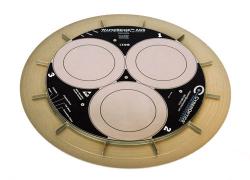
 CyberOptics' Auto Gapping System
Besides delivering inaccurate measurements, it was also hazardous and exposed particles to pollution since users continuously opened and closed the heated PECVD compartment.
The AGS is a secure and accurate gapping technique that minimizes time needed for the process. It has been configured with three capacitive detectors in a wafer-thin footprint. It determines the distance to a conductive electrode at three spots on the showerhead and transmits rapid gap calculations to a GUI. Additional software helps transmit data as a CSV file.
It eliminates exposure to pollutants and helps the technicians determine multiple potential gaps and pre-fixed gaps accurately up to a thousandth of an inch for compact film deposition and manufacture tolerances at 300mm fab. Having tested the wireless gapping technique over a two month period, the scientists established that the wireless technique with its time-efficient maintenance of the PECVD chamber’s gap settings, reduced it from 10 to 4 hours or less, a lessening of 60%.
Source: http://www.CyberOpticsSemi.com
Please use one of the following formats to cite this article in your essay, paper or report:
APA
Chai, Cameron. (2019, February 12). WaferSense Auto Gapping System to Help 300 mm fab Boost Accessibility of PECVD Tool. AZoNano. Retrieved on March 23, 2026 from https://www.azonano.com/news.aspx?newsID=21976.
MLA
Chai, Cameron. "WaferSense Auto Gapping System to Help 300 mm fab Boost Accessibility of PECVD Tool". AZoNano. 23 March 2026. <https://www.azonano.com/news.aspx?newsID=21976>.
Chicago
Chai, Cameron. "WaferSense Auto Gapping System to Help 300 mm fab Boost Accessibility of PECVD Tool". AZoNano. https://www.azonano.com/news.aspx?newsID=21976. (accessed March 23, 2026).
Harvard
Chai, Cameron. 2019. WaferSense Auto Gapping System to Help 300 mm fab Boost Accessibility of PECVD Tool. AZoNano, viewed 23 March 2026, https://www.azonano.com/news.aspx?newsID=21976.
We're committed to providing free access to quality science. By registering and providing insight into
your preferences you're joining a community of over 1m science interested individuals and help us to
provide you with insightful content whilst keeping our service free.
or
Terms
While we only use edited and approved content for Azthena
answers, it may on occasions provide incorrect responses.
Please confirm any data provided with the related suppliers or
authors. We do not provide medical advice, if you search for
medical information you must always consult a medical
professional before acting on any information provided.
Your questions, but not your email details will be shared with
OpenAI and retained for 30 days in accordance with their
privacy principles.
Please do not ask questions that use sensitive or confidential
information.
Read the full Terms & Conditions.