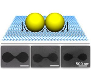
A team led by Enge Wang and Wenlong Wang researching at the Beijing National Laboratory for Condensed Matter Physics and Peking University has developed a scalable technique to develop graphene nanoribbons.
The research paper is titled, ‘Nanosphere Lithography for the Fabrication of Ultra narrow Graphene Nanoribbons and On-Chip Bandgap Tuning of Graphene’.
 PKU's Sphere-based Etching of Graphene sheets
A sheet of graphene sheet was altered with 1µm polysterene spheres to create graphene ribbons that automatically aligned themselves in tight arrays. The sample was then etched with oxygen plasma. The plasma ions are dispersed between the spheres. The etching made patterns on the grapheme in complicated shapes such as dumbbell, ribbon networks, linear and circular chains, and polygonal rings. When the spheres were washed, the various patterns could be collected. The team was able monitor the etching time, and also the sphere packing to help develop specific patterns.
The thin strips of graphene displayed a bandgap enabling their use in electronic components. The team developed a transistor using a graphene sheet and etched the graphene with a polystyrene bead-based technique. The transistor did not exhibit transistor function before being etched, but displayed it after the procedure for 30 seconds, exhibiting an on–off ratio of 90 for current switching. The transistor channel conductivity was lowered.
The cost- effective fabrication method is easy to emulate and can create multiple graphene nanoribbons simultaneously. It can also help alter and repair finished products.