Researchers at the National Institute of Standards and Technology (NIST) and the Georgia Institute of Technology have published a paper in the Physical Review B journal describing the probable occurrence of a family of seven defect structures in graphene sheets. They have also produced images of the low-energy defects that appear in the family.
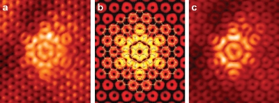
 Flower-like defects in graphene are shown in these images (a and b) produced by a scanning tunneling microscope. Image b was created by a computer model.
The defects may arise to alleviate mechanical stress present in the honeycomb structure of graphene by allowing atoms to disperse and take up relatively more space. Such stress originates during growth of the graphene sheet or due to stretching. In the case of electronic applications, the defects could change the path of electrons and result in backscattering that would increase the material’s resistance. Phillip First, a co-author of the paper, says superior growth methods established during the defect study may help to overcome this concern.
Joseph Stroscio, a NIST Fellow, stated that defects can originate when carbon atoms move at high temperatures. Minimal amount of energy is required to rearrange graphene from a six-member carbon ring to contain only five or seven atoms. NIST researchers have found that a grain boundary loop or a new type of defect can be introduced in the honeycomb structure by holding rings of five and seven-member rings together in closed loops.
According to Eric Cockayne, a NIST researcher, the fabrication process results in formation of defects. Researchers have observed only the flower defect which comprises six pairs of five- and seven-atom rings. Graphene’s atomic structure has been modeled by the NIST team suggesting that a bouquet of flower-like arrangements may actually exist. Cockayne stated that the flower-like defects numbering to seven will have a unique set of electrical and mechanical properties.