Graphene, one atom thick pure carbon lattice with amazing strength, electrical and thermal conductivity lacks one key property.
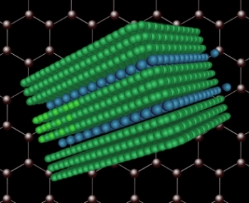
 bromine or chlorine (represented in blue) are introduced into a block of graphite (shown in green)
It does not have the ability to create a band gap, which is a specific energy range that exists between bands to enable the existence of electrons. The band gap is necessary for devices such as computer chips, transistors, and solar cells.
MIT scientists have identified a method to produce considerable quantities of two or three layer graphene. When the layers are arranged in a specific manner, these structures render graphene the needed band gap. Nature Nanotechnology journal has published a paper describing the new method.
Michael Strano, associate professor of Chemical Engineering, MIT, stated that this new technique enables high-precision arrangement of graphene layers by centering the atoms existing in one layer over the space present between atoms in the other layer. This arrangement is known as A-B stacked that offers needed electronic properties to graphene.
Chlorine or bromine compounds injected into a graphite block naturally enters the material structure, accommodating themselves in a specific pattern either between each layer, or even every third layer, causing the layers to move away from each other. Strano and his team discovered that on dissolving graphite, it disintegrates at the place having the added atoms, creating two or three layer thick graphene flakes. This mild dispersion method may result in larger flakes of graphene than obtained in other methods. Since graphene is a delicate material, processing needs to be very mild.
This method produces large flakes about 50 mm2 enabling applications for electronic and optoelectronic devices, for example the team produced few simple transistors using the material.