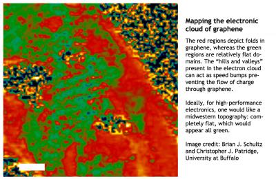
Chemists at the University at Buffalo made use of synchrotron light to monitor the electron clouds on graphene’s surface. They revealed with the help of a series of images how ripples and folds in graphene can hamper its conductivity.
 The red regions depict folds in graphene, whereas the green regions are relatively flat domains
Graphene has a unique structure that enhances its conductive properties. Under normal conditions, when graphene is entirely flat, electric charges can travel at quick rates without facing many barriers, stated Sarbajit Banerjee, a researcher at UB who led the research in Nature Communications. It is important to note that conditions are not optimal always.
The images captured by Banerjee and his coworkers demonstrate that when graphene is in the bent or folded state, the electron cloud along its surface gets warped, thus making it more challenging for an electric charge to pass through.
A staff scientist at the Molecular Foundry at Berkeley Lab, David Prendergast, stated that with the help of simulations it is possible to comprehend the measurements made using X-rays, and to estimate how small changes in graphene’s structure can alter its electronic properties. He added that they observed that certain areas of graphene were sloped at various angles.
The research team documented how graphene folds distorted its electron cloud. In addition, they found that pollutants that adhere to graphene settle in valleys where the graphene surface is not uniform. Such pollutants affect the electron cloud, thus varying the strength with which the cloud is attached to the basic atoms.
Graphene's unique properties will be useful in industries such as energy, computing and defense. Scientists claim that graphene exhibits electrical conductivity equivalent to copper.
The UB-led research suggests that organizations wanting to integrate graphene into products such as ultrafast transistors, conductive inks, and solar panels could conduct more research on the nanomaterial. To increase the performance of commercial products flat sheets of graphene can be transferred onto them.