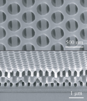
A MIT research team has identified a new hybrid method to produce more complex nanostructured materials (three-dimensional nanostructures) by combining top-down and bottom-up approaches.
 The new 3D nanofabrication method makes it possible to manufacture complex multi-layered solids all in one step.
A top-down approach also known as phase-shift lithography is one in which a two-dimensional mask patterns the light intensity directed on a photoresist material layer similar to how a photographic negative manipulates the amount of light focused on different print areas. The photoresist is modified only at the areas exposed to light. By this method, it is essential to accurately produce phase masks that consume more cost and time.
The bottom-up approach uses self-arranging colloidal nanoparticles that assemble themselves into a close-packed structure. These structures can be used as a mask for physical deposition methods, which include vapor deposition or surface etching, to form two-dimensional structures. However, the two methods are slow and may cause faults in the three-dimensional layers.
The new method is a combination of these two approaches, in which the self-assembled layers are created directly on a substrate that acts as a mask during the lithography process. Each individual nanoparticle, arranged on the surface, behaves as a tiny lens that directs the light rays into an intensity pattern based on their surface arrangement.
Members of the team who specialize in optics stated that they are planning to produce photonic crystals that are arranged in such a way that can control the light beam that passes through them. Additionally, this technique can be applied to make phononic materials, which can manipulate sound or heat waves and to form filters with accurately controlled porosity for usage in biomedical applications.