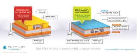
"We are now producing NanoEMS sensors in volume in a standard CMOS production line." said Dave Doyle, Baolab's CEO. "The move from lab to fab is a significant milestone for the company, proving that our innovative technology is reliable, scalable and repeatable. This was the critical stage that our customers have been waiting for. NanoEMS makes it much easier and more cost effective to integrate MEMS sensors with microcontrollers and associated electronics all on the same chip in the same CMOS production line. This is the breakthrough that will enable high volume, consumer electronics products to have intelligent sensors, meeting the increasing demand for smarter, more aware devices."
NanoEMS technology not only offers significant cost reductions in motion MEMS sensors but Baolab envisages the possibility for NanoEMS structures to be easily incorporated into ASICs for applications such as RF Antennas, RF switches, Near Field Communications and Automotive. Possible areas that Baolab and its customers are investigating are:-
Vibrating antennas
These overcome the limitations of classic (static) antennas such as compact superdirective/superesolution antennas/lenses that require phase shifters and gains with an accuracy not currently realistic. Vibrating antennas make these feasible along with spatial multiplexing communications for mobile telecoms and internet.
Thermo-magnetic RF switches & antennas
By exploiting the low value of the Curie temperature of Nickel, it is possible to build RF switches, filters and reconfigurable antennas. This creates a novel category of reconfigurable RF MEMS components which are highly reliable, since there are no moving parts, achieving compelling RF specs, low power consumption and low cost thanks to CMOS processing.
Modal switches
This novel topology enables compelling specifications for RF switches with low-capacitance ratio and high isolation, using low cost, low resistivity CMOS substrates. The principle is based on transferring power from the different transmission modes in a transmission line, using reconfigurable MEMS loads to balance and unbalance the line.
Integrated passives: inductors, transformers, capacitors
Integrated inductors with a helicoidal shape typical of off-chip inductors, offer reduced losses (higher Q) and smaller parasitic capacitance (higher resonant frequency). It is also possible to create transformers with any winding ratio.
Integrated capacitors for low frequency applications, especially power, where the tangent capacitance is used instead of the traditional approach using secant capacitance. When capacitors are used in voltage regulators, only a small fraction of the charge stored in the capacitor is typically used to regulate the voltage. This kind of capacitor allows a higher percentage of the stored charge to be used to regulate the voltage, which makes it possible to implement smaller, integrated filters and regulators, with superior performance.
RF filters
The small feature size of CMOS processing makes it is possible to implement RF MEMS filters up to the GHz band required for cell phone communications and significantly increase the electromechanical coupling. Current MEMS RF mechanical filters have a problem with very low electromechanical coupling, which means low sensitivity, that they try to offset by means of using a very high voltage but with limited success.
Power converters
NanoEMS MEMS enable integrated charge pumps and power supplies, which are lower in cost, more compact and more efficient.
