Cascade Microtech Unveils New Integrated Solution for On-Wafer Power Device Test
Wafer level precision measurement solution provider, Cascade Microtech has unveiled its new and the industry’s first fully automatic measurement solution for high power devices at the wafer level.
 APS200TESLA
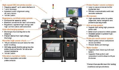
Labeled APS200TESLA, the device combines the capabilities of the company’s BlueRay production automation technology and Tesla on-wafer characterization measurement of power device technology.
The rise in demand for environment-friendly and energy-efficient power devices is expected to trigger a shift in manufacturing of power semiconductors from employing silicon substrates to employing gallium nitride (GaN), silicon carbide (SiC) and gallium nitride on silicon (GaN-on-Si). The new semiconductor substrate technology, which finds application in areas such as electrical power distribution, consumer and automotive electronics in the form of switching devices such as MOSFETs and IGBTs, offers faster switching and high power capabilities and improves efficiency of the power devices. This poses a challenge to power device manufacturers to identify test solutions that facilitate the measurement of high power devices. The APS200TESLA addresses this problem by facilitating high-current and high-voltage device characterization at the wafer level by means of a high-voltage/high-power chuck port, a high-voltage/high-current probe card and the yet to be patented MicroVac high-power chuck capable of handling as low as 50 µm thickness.
The on-wafer testing reduces the time to market and reduces test costs by eliminating the need for dicing and packaging before testing. The device can be interfaced with a host of test instruments via electrical connection. The arc-suppression element allows for flexibility in designing device layout for optimum yield. Safety features such as safety shield to protect operators and damage prevention from high-voltage discharge by auto-discharging and sensing capability through probe pins are incorporated in the device.
Written by
Will has a B.Sc. in Chemistry from the University of Durham, and a M.Sc. in Green Chemistry from the University of York. Naturally, Will is our resident Chemistry expert but, a love of science and the internet makes Will the all-rounder of the team. In his spare time Will likes to play the drums, cook and brew cider.
Please use one of the following formats to cite this article in your essay, paper or report:
APA
Soutter, Will. (2019, February 12). Cascade Microtech Unveils New Integrated Solution for On-Wafer Power Device Test. AZoNano. Retrieved on April 07, 2026 from https://www.azonano.com/news.aspx?newsID=24992.
MLA
Soutter, Will. "Cascade Microtech Unveils New Integrated Solution for On-Wafer Power Device Test". AZoNano. 07 April 2026. <https://www.azonano.com/news.aspx?newsID=24992>.
Chicago
Soutter, Will. "Cascade Microtech Unveils New Integrated Solution for On-Wafer Power Device Test". AZoNano. https://www.azonano.com/news.aspx?newsID=24992. (accessed April 07, 2026).
Harvard
Soutter, Will. 2019. Cascade Microtech Unveils New Integrated Solution for On-Wafer Power Device Test. AZoNano, viewed 07 April 2026, https://www.azonano.com/news.aspx?newsID=24992.
We're committed to providing free access to quality science. By registering and providing insight into
your preferences you're joining a community of over 1m science interested individuals and help us to
provide you with insightful content whilst keeping our service free.
or
Terms
While we only use edited and approved content for Azthena
answers, it may on occasions provide incorrect responses.
Please confirm any data provided with the related suppliers or
authors. We do not provide medical advice, if you search for
medical information you must always consult a medical
professional before acting on any information provided.
Your questions, but not your email details will be shared with
OpenAI and retained for 30 days in accordance with their
privacy principles.
Please do not ask questions that use sensitive or confidential
information.
Read the full Terms & Conditions.