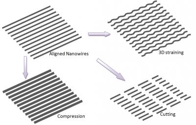
Researchers at the Purdue University have developed a novel "nano machine shop" that can be used for shaping ultrathin films and nanowires.

This illustration depicts a new "nano machine shop's" ability to shape tiny wires, an advance that represents a possible future manufacturing method for tiny structures with potentially revolutionary properties. Credit: Gary Cheng, Purdue University
The new method holds potential for manufacturing tiny structures with special properties such as "plasmonic resonance" and ultrahigh magnetism.
The novel technique called laser shock-induced shaping was used to stamp microgears and nanogears, and tiny shapes out of graphene, and for modifying the shape of silver nanowires. The fabrication was conducted at atmospheric pressure and room temperature conditions. The researchers demonstrated how the laser shock-induced shaping method may be used for modifying the properties of graphene, which may enable utilizing the material for potential electronic applications.
Nanowires are thin filaments that are 1,000 times thinner than a human hair. They hold potential for being used in many applications, but they have to be modified for the specific applications. This modification requires appropriate technologies. The laser shock-induced shaping technology enables tuning of nanowires by changing its optoelectrical and electrical properties. This modification will allow it to be used for electronic instruments and components.
The manufacturing method involves a using a multilayered sandwich structure with a tiny mold located at its bottom. Nanowires are located over this tiny mold. In between these nanowires and a glass cover sheet various other materials are layered. An ultra-fast pulsing laser burns up a layer when the layered "forming unit" is exposed to it. This causes a downward pressure that pushes the nanowires into the tiny mold leading to a modification in its shape.
The cost-effective and quick method can be scaled up for industrial level processing.
The study has been published in the journal Nano Letters and highlighted in the journal Nature Photonics.
Disclaimer: The views expressed here are those of the author expressed in their private capacity and do not necessarily represent the views of AZoM.com Limited T/A AZoNetwork the owner and operator of this website. This disclaimer forms part of the Terms and conditions of use of this website.