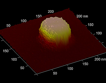
National Institute of Standards and Technology (NIST) has devised a hybrid metrology technique that could reduce the uncertainties related to the measurement of features on the computer chip. The hybrid metrology technique is a combination of statistical analysis and scanning techniques.
 This tiny silicon pillar, measuring less than 100 nanometers along any of its sides, is the sort of computer chip feature that manufacturers now can measure more precisely with NIST’s hybrid metrology method, which can reduce the nagging uncertainties that have long plagued industry’s measurement efforts. Credit: NIST
The process of manufacturing a computer chip involves a lot of uncertainty, especially while dealing with the measurement of nanometer-sized features. Optical microscopes cannot effectively analyze these small features. Metrologists generally use other methods such as atomic force microscopy (AFM) and scatterometry to study these features.
In scatterometry, the light scattered from the edges of the computer chip creates a pattern from which feature properties can be deduced. In cases where scatterometry is not effective, metrologists use AFM, a slow and expensive process by which a nano-sized object’s width and height can be measured.
Richard Silver, a scientist at NIST, said that if the width of an object is calculated to be 40 nm using scatterometry, the actual width would vary more or less by 3 nm. He feels this variance is relatively large, and moreover, uncertainties could increase when other techniques of measurement are combined, leading to lesser clarity. He also said that GLOBALFOUNDRIES and IBM have started employing the hybrid metrology technique, after it was introduced through a conference in 2009, and have been successful.
Scientists from NIST tried to work on devising a technique that was more accurate and economical. The measurements obtained from AFM and scatterometry methods were compared with simulated data stored in a library. However, this too had a high level of uncertainty. Nien Fan Zhang, a statistician with NIST, employed Bayesian analysis and incorporated a few more measured values into the previous library model. This approach reduced uncertainties to a great extent in a few cases.