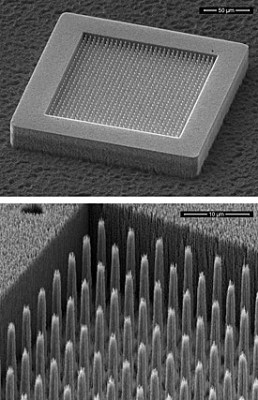
Scientists at the National Institute of Standards and Technology (NIST) and the University of Maryland, College Park, have built a practical, high-efficiency nanostructured electron source. Described in the journal Nanotechnology, this new, patent-pending technology could lead to improved microwave communications and radar, and more notably to new and improved X-ray imaging systems for security and health-care applications.
 NIST's silicon carbide field emitter produces a flow of electrons comparable to hot sources, but without the need for heat. By dissolving much of the material away to make a porous structure with a large surface area, NIST scientists ensured that as an electron emission point on an individual spike wears out, another is available to take its place, making the array more durable as a whole. Credit: Sharifi/NIST
While thermionic electron sources such as the hot filaments inside cathode ray tubes have largely been replaced by LEDs and liquid crystals for display screens and televisions, they are still used to produce microwaves for radar and X-rays for medical imaging. Thermionic sources use an electric current to boil electrons off the surface of a wire filament, similar to the way an incandescent light bulb uses an electric current to heat a wire filament until it glows.
And like an incandescent light bulb, thermionic sources are generally not very energy efficient. It takes a lot of power to boil off the electrons, which spew in every direction. Those that aren't lost have to be captured and focused using a complicated system of electric and magnetic fields. Field emission electron sources require much less power and produce a much more directional and easily controllable stream of electrons.
To build their field emission source, the NIST team took a tough material—silicon carbide—and used a room-temperature chemical process to make it highly porous like a sponge. They then patterned it into microscopic emitting structures in the shape of pointed rods or sharp-edged fins. When an electric field is applied, these novel field emitters can produce an electron flow comparable to a thermionic source but without all the disadvantages—and with many advantages.
According to co-inventor Fred Sharifi, the new field emitters have inherently fast response times compared with thermionic sources, and the absence of heat makes it easier to create arrays of sources. Moreover, the porous nanostructure of the emitters makes them very reliable. Even if the emitter surface wears away during use—a common problem—the newly exposed material continues to work just as well.
Sharifi says that the NIST field emitters hold the potential to enhance the resolution and quality of X-ray images and allow for new modes of detection.
"X-ray images are based on the density of the material being examined, which limits their ability to see certain types of materials, including some types of explosives," says Sharifi. "Our field emitter will let us see not just that something is there, but, because we can build large arrays and place them at different angles, we can identify the material in question by looking at how the X-rays coming from different directions scatter from the object."
The technology is available for licensing through NIST's Technology Partnerships Office.