Jun 28 2013
For the first time, a team of researchers at the HZB led by Dr. Roland Mainz and Dr. Christian Kaufmann has managed to observe growth of high-efficiency chalcopyrite thin film solar cells in real time and to study the formation and degradation of defects that compromise efficiency.
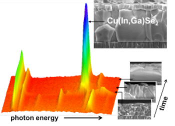
 Polycrystalline film growth during coevaporation in real time using in situ X-ray diffraction and fluorescence analysis. Figure: R. Mainz/C.Kaufmann/HZB
To this end, the scientists set up a novel measuring chamber at the Berlin electron storage ring BESSY II, which allows them to combine several different kinds of measuring techniques. Their results show during which process stages the growth can be accelerated and when additional time is required to reduce defects. Their work has now been published online in Advanced Energy Materials.
Today’s chalcopyrite thin film cells based on copper indium gallium selenide are already reaching efficiencies of more than 20 percent. For the fabrication of the extremely thin polycrystalline layers, the process of coevaporation has lead to the best results so far: During coevaporation, two separate elements are evaporated simultaneously, first indium (or gallium) and selenium, then copper and selenium, and, finally, indium (or gallium) and selenium again. This way, a thin film of crystals forms, which exhibit only a small number of defects. “Until recently, we did not fully understand what exactly happens during this coevaporation process,” says Dr. Roland Mainz of the HZB’s Institute of Technology. The team of physicists worked for three years using on-site and real-time measurements to find an answer to this question.
Novel experimental chamber constructed
For these measurements they constructed a new kind of experimental chamber, which allows for an analysis of polycrystalline chalcopyrite film formation during coevaporation when exposed to synchrotron light at BESSY II. In addition to the evaporation sources for the elements, this vacuum chamber contains heating and cooling elements to control the evaporative process. According to Mainz, “one of the main challenges was adjusting the chamber, which weighs around 250 kilograms, with an accuracy of 10 micrometer.” Because of thermal expansion during evaporation, the height has to be automatically re-adjusted every few seconds.
Combination of x-ray diffraction and fluorescence analysis
With this setup, for the first time worldwide they were able to observe polycrystalline film growth using in situ X-ray diffraction and fluorescence analysis during coevaporation in real time. “We are now able to see how crystalline phases form and transform and when defects form during the different stages of evaporation. “But we’re also able to tell when these defects disappear again.” This takes place in the second process stage, when copper and selenium are evaporated. Excess copper, which deposits at the surface in the form of copper selenide helps to remove defects. “This was already known before from previous experiments. But now, using fluorescence signals and numeric model calculations, we are able to show how copper selenide penetrates the copper indium selenide layer,” Mainz explains. Here clear-cut differences between copper indium selenide and copper gallium selenide layers became apparent: While copper is able to penetrate the copper-indium-selenide layer, in the case of copper-gallium-selenide, which is otherwise pretty similar, it remains at the surface. This could be one possible reason for why the use of pure copper gallium selenide does not yield high efficiency solar cells.
Concrete steps for optimization
“We now know that for further optimization of the process it is important to concentrate on the transition point into the copper-rich phase. Up to now the process was performed very slowly throughout all stages to give defects enough time to disappear. Our findings suggest that the process can be accelerated at some stages and that it is sufficient to slow it down only at points where defects are efficiently eliminated,” explains Mainz. Mainz is already looking forward to future project EMIL, which is currently being set up at BESSY II. Here even more powerful tools will become available for the study of complex processes during growth of new types of solar cells in situ and in real time.
Read the original paper in Advanced Energy Materials here: http://dx.doi.org/10.1002/aenm.201300339