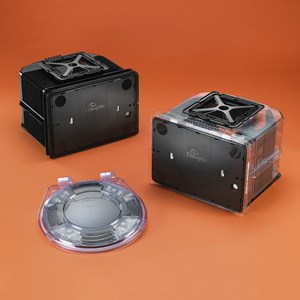
Entegris, Inc., a leader in yield-enhancing materials and solutions for highly advanced manufacturing environments, announced the release and global availability of their next generation of 450 mm wafer carrier solutions (P2) for the safe and reliable transport of 450 mm wafers used in semiconductor manufacturing.

The 450 mm P2 wafer carriers enable customers to efficiently ship and process SEMI® M1 standard wafers through precise alignment with 450 mm equipment standards, low particle generation, and reduced cleaning cycle time.
"As the industry transitions to 450 mm, manufacturers are facing new wafer handling challenges to maintain the level of cleanliness required to produce SEMI standard M1 quality wafers," said Todd Edlund, senior vice president and chief operating officer of Entegris. "Entegris has been closely collaborating with leading silicon suppliers and OEMs to expand the shipment and processing of 450 mm wafers. As part of these collaborations, we have shipped our 450 mm wafer handling solutions to more than 50 critical industry players."
The 450 mm P2 Multiple Application Carriers (MAC) and 450 mm Front Opening Unified Pod (FOUP) have been extensively tested by the Global 450 mm Consortium (G450C) in Albany, New York at SUNY Polytechnic Institute. With this collaboration, Entegris has improved the architecture of the MAC and FOUP carriers to ensure seamless equipment interoperability within the fab. Dave Skilbred, Director of Program Coordination/Management at G450C said, "The launch of the 450 mm P2 MAC and FOUP clearly demonstrates Entegris' leadership and commitment to support the industry transition to M1 450 mm wafer quality and to continue to advance progress on fully patterned 450 mm wafers."
With robust sealing and an optimized mechanism for "capturing" the wafer as it enters the carrier, the P2 MAC delivers a cleaner wafer environment with improved protection from handling and environmentally induced particle generation. The 450 mm wafer carrier design also reduces the cleaning cycle time by 25-50% for increased fab efficiency. In addition, the 450 mm P2 MAC shipping system has been tested to meet both MAC and FOSB SEMI standards of performance.