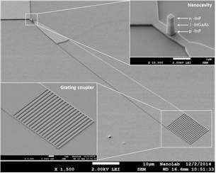
The nanoLED SEM image (pictured) by Eindhoven University of Technology (TU/e) recently won a competition held by Oxford Instruments Plasma Technology, and chosen from a large number of entries, all demonstrating unique and intriguing process results obtained using Oxford Instruments equipment.
Submitted by PhD Candidate Victor Dolores-Calzadilla from the Photonic Integration Group at TU/e, the SEM image titled “Integrated nanoLED for photonic circuits” was achieved using a combination of three Oxford Instruments plasma processing tools.

The SEM image clearly demonstrates the cutting edge plasma etch and deposition technology that Oxford Instruments Plasma Technology’s systems offer the LED fabrication market.
Dolores-Calzadilla states:
“We’re currently researching metal-cavity nanolasers and nanoLEDs using Oxford Instruments systems for their fabrication. This nanoLED is just one example of the excellent results we are achieving using a combination of Oxford Instruments Plasmalab®100 RIE, ICP and PECVD tools. I am thrilled with our results and am happy to demonstrate the capabilities of the Photonic Integration Group at TU/e.”
Dr David Haynes, Sales, Marketing & CS Director at Oxford Instruments Plasma Technology comments:
“We are delighted to showcase the work of our customers, and to view the intricate processes produced with our systems. This competition was a fantastic insight into the multiple uses of our technology, and we were pleased to receive so many diverse entries.”
Victor Dolores-Calzadilla won £150 in Amazon vouchers for his entry.
Full information on how the nanoLED SEM was created can be found on the Oxford Instruments website:
www.oxford-instruments.com/SEM-2015
About Oxford Instruments Plasma Technology
Oxford Instruments Plasma Technology offers flexible, configurable process tools and leading-edge processes for the precise, controllable and repeatable engineering of micro- and nano-structures. Our systems provide process solutions for the etching of nanometre sized features, nanolayer deposition and the controlled growth of nanostructures.
These solutions are based on core technologies in plasma-enhanced deposition and etch, ion-beam deposition and etch, atomic layer deposition, deep silicon etch and physical vapour deposition. Products range from compact stand-alone systems for R&D, through batch tools and up to clustered cassette-to-cassette platforms for high-throughput production processing.