Oct 31 2015
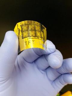
Inspired by mammals' eyes, University of Wisconsin-Madison electrical engineers have created the fastest, most responsive flexible silicon phototransistor ever made.
 Developed by UW-Madison electrical engineers, this unique phototransistor is flexible, yet faster and more responsive than any similar phototransistor in the world. Credit: Jung-Hun Seo
The innovative phototransistor could improve the performance of myriad products -- ranging from digital cameras, night-vision goggles and smoke detectors to surveillance systems and satellites -- that rely on electronic light sensors. Integrated into a digital camera lens, for example, it could reduce bulkiness and boost both the acquisition speed and quality of video or still photos.
Developed by UW-Madison collaborators Zhenqiang "Jack" Ma, professor of electrical and computer engineering, and research scientist Jung-Hun Seo, the high-performance phototransistor far and away exceeds all previous flexible phototransistor parameters, including sensitivity and response time.
The researchers published details of their advance this week in the journal Advanced Optical Materials.
Like human eyes, phototransistors essentially sense and collect light, then convert that light into an electrical charge proportional to its intensity and wavelength. In the case of our eyes, the electrical impulses transmit the image to the brain. In a digital camera, that electrical charge becomes the long string of 1s and 0s that create the digital image.
While many phototransistors are fabricated on rigid surfaces, and therefore are flat, Ma and Seo's are flexible, meaning they more easily mimic the behavior of mammalian eyes.
"We actually can make the curve any shape we like to fit the optical system," Ma says. "Currently, there's no easy way to do that."
One important aspect of the success of the new phototransistors is the researchers' innovative "flip-transfer" fabrication method, in which their final step is to invert the finished phototransistor onto a plastic substrate. At that point, a reflective metal layer is on the bottom.
"In this structure -- unlike other photodetectors -- light absorption in an ultrathin silicon layer can be much more efficient because light is not blocked by any metal layers or other materials," Ma says.
The researchers also placed electrodes under the phototransistor's ultrathin silicon nanomembrane layer -- and the metal layer and electrodes each act as reflectors and improve light absorption without the need for an external amplifier.
"There's a built-in capability to sense weak light," Ma says.
Ultimately, the new phototransistors open the door of possibility, he says.
"This demonstration shows great potential in high-performance and flexible photodetection systems," says Ma, whose work was supported by the U.S. Air Force. "It shows the capabilities of high-sensitivity photodetection and stable performance under bending conditions, which have never been achieved at the same time."