Jun 14 2016
Wafer-scale and high yield synthesis has been realized by a team of researchers from Tohoku University. As per the research conducted at Hokkaido University and the University of Tokyo, the comparison of molecular dynamics simulations, experiments and theoretical calculations has illuminated the distinctive growth dynamic.
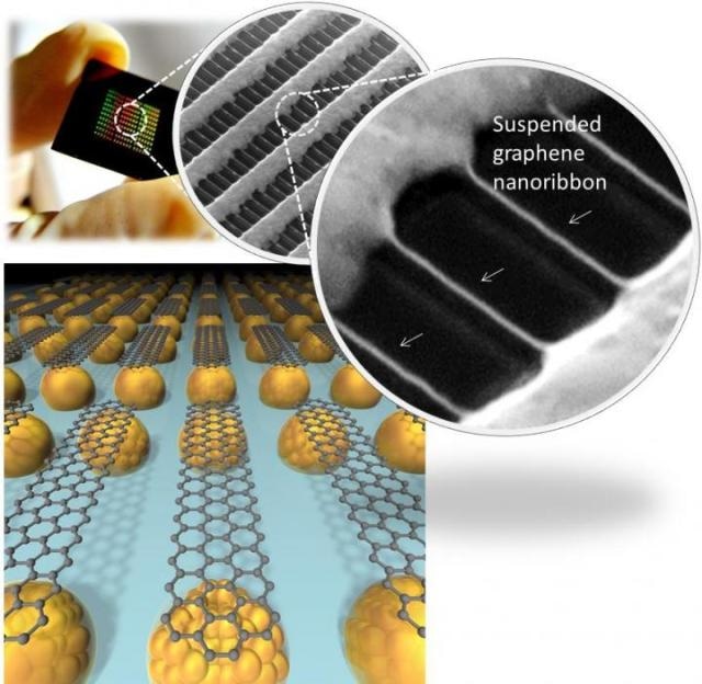
 Suspended graphene nanoribbons in wafer-scale. (Photo credit: Toshiaki Kato)
When a mechanical degree of freedom is added to optical and electrical properties of atomically thin materials, it helps in achieving an outstanding platform to inspect a wide range of optoelectrical physics and devices with mechanical motion interaction. The challenging part is the fabrication of atomically thin materials with suspended structures on a massive scale.
A bottom-up approach has been used by the team of researchers, headed by Associate Prof. Toshiaki Kato, to illustrate wafer-scale, high-yield synthesis of suspended graphene nanoribbon, and this in turn brought the growth dynamics to limelight. There is a possibility of combining about 1,000,000 suspended graphene nanoribbons in wafer-scale substrate leading to an increase in the yield by more than 90%.
Shaping atomically thin materials in suspended structures may provide a viable platform for nanoscale mechanical oscillators.
Toshiaki Kato, Associate Professor, Tohoku University
Strips of graphene with quasi 1D structure are known as graphene nanoribbon (width ∼ a few tens nm, length, ∼ few µm). Graphene nanoribbons are different from 2D graphene and they include a band gap based on the edge and width structures. It is predicted that advanced high performance optoelectrical semiconductor applications can make a use of these graphene nanoribbons.
Kato further adds that, "The actualization of high yield and wafer-scale synthesis of suspended graphene nanoribbon will have an impact on the study of graphene nanoribbon, and be used in practical applications in a wide variety of fields."
The particulars about this study can be found online in Nature Communications (June 2).