Physicists from MIPT and Skoltech have found a way to modify and purposely tune the electronic properties of carbon nanotubes to meet the requirements of novel electronic devices. The paper was published in the Carbon journal.

Nanotube films. Image Credit: Elena Khavina/MIPT
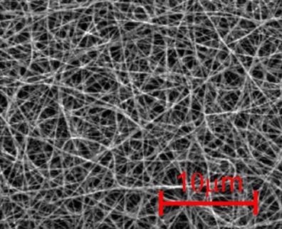
Carbon nanomaterials form an extensive class of compounds that includes graphene, fullerenes, nanotubes, nanofibers, and more. Although the physical properties of many of these materials already appear in textbooks, scientists continue to create new structures and find ways to use them in real-life applications. Macro structures designed as randomly oriented films made of carbon nanotubes look like very thin cobwebs with an area reaching several dozen square centimeters and thickness of only a few nanometers.

Figure 1. Carbon nanotube film under a scanning electron microscope. Image Credit: MIPT & Skoltech

Figure 2. Oxygen plasma treatment creates defects that change electrical characteristics of carbon nanotubes (left). The top box shows surface resistance versus frequency for treated (red curve) and pristine (blue curve) films (right). The lower box shows temperature coefficients of resistance (TCR) versus temperature for the same films. Image Credit: MIPT & Skoltech
Carbon nanotube films display an amazing combination of physical and chemical properties, such as mechanical stability, flexibility, stretchability, excellent adhesion to various substrates, chemical inertness, and exceptional electrical and optical properties.
Unlike metallic films, these highly conducting films are light and flexible and, therefore, can be used in various electrical devices, such as electromagnetic shields, modulators, antennas, bolometers, and so on.
The knowledge of the underlying physical principles is essential for the effective use of the films’ electrical and electrodynamic properties in real life. Of particular interest are the terahertz and far-infrared spectral bands with wavelengths of 2 mm to 500 nm where the films exhibit properties typical for metallic conductors.
MIPT and Skoltech scientists studied films conductivity in the terahertz and infrared bands using films synthesized by the gas phase deposition method. Some of the films were made of nanotubes with lengths varying from 0.3 to 13 µm, while others were treated with oxygen plasma for 100 to 400 seconds and changed their electrodynamic properties in the process.
In an earlier study, the authors proved that conductivity of high-quality pristine films can be accurately described using the conductivity model valid for metals. In these films, free electrons have enough energy to overcome potential barriers at the intersections of individual nanotubes and can move quite easily over the entire film, which results in high conductivity.
However, shortening tubes length (down to 0.3 μm) or exposing films to plasma (for longer than 100 s) leads to a drop in conductivity at low terahertz frequencies (< 0.3 THz). The team discovered that in both cases conductivity changes in much the same way and produces similar results. Exposure to plasma results in a larger amount of defects and, therefore, a larger amount of potential barriers for itinerant electrons. For shorter nanotubes, the number of barriers per unit area increases, too. The barriers strongly affect the conductivity of both nanotubes and films at direct current (DC) and fairly low frequencies, because at low temperatures electrons lack kinetic energy to overcome potential barriers. The authors showed that at high enough frequencies electrons move freely as if the barriers were not there. At low frequencies and in the DC case, films made up of short or plasma-treated tubes exhibit a higher temperature coefficient of resistance (TCR) which shows how resistance changes with temperature.
For plasma exposure of over 100 seconds or nanotube lengths below 0.3 μm, TCR reaches saturation. The effect can be considered as a precursor of TCR reduction in the films that are exposed to plasma for a very long time when separate tubes become severely damaged and lose their peculiar electric properties.
MIPT and Skoltech researchers plan to continue studying modified films, including those stretched in one or more directions. Boris Gorshunov, a co-author of the paper and head of the MIPT Laboratory of Terahertz Spectroscopy, comments:
In contrast to nanotubes that have long been studied in great detail, research on macro objects, such as nanotube films, started only recently. Nanotube films are much lighter and more stable chemically and mechanically than metallic films and, therefore, are more appealing for electronics applications. Since we know the fundamental physics behind the films’ electrical properties, we can tune them for specific real-life applications. Research in the terahertz band which will soon become ubiquitous in telecommunications is of particular relevance.
“It turned out that controlled destruction of this remarkable material by microwave plasma results in a series of surprising properties, such as a noticeable increase in TCR in films made of single-walled carbon nanotubes. This happens because the competing contributions of metallic and semiconductor tubes to conductivity no longer play an important role, and the film conductivity is determined primarily by the amount of defects. This feature is highly interesting for the design of new generation devices, such as room-temperature high-speed bolometers,” professor Albert Nasibulin, head of the Laboratory of Nanomaterials at Skoltech, notes.