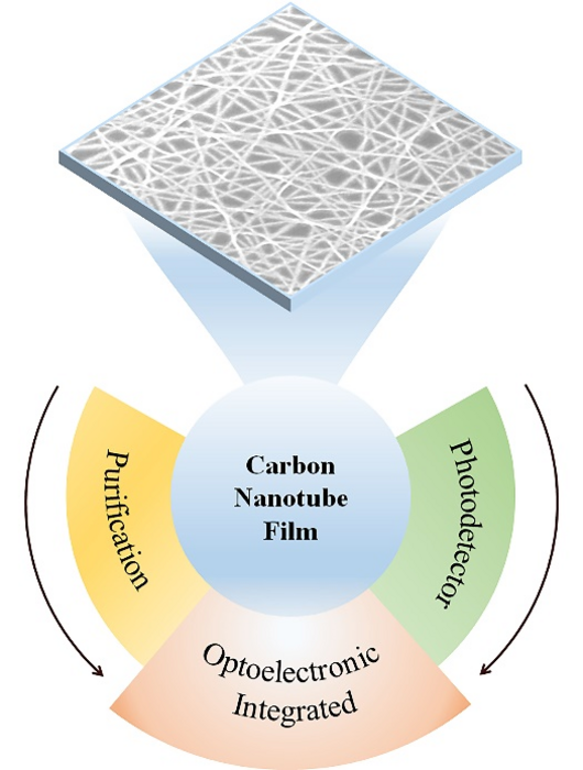
With additional optimization and research, highly purified semiconducting single-walled carbon nanotube (s-SWCNT) films will exceed current photodetector performance and efficiency at a significantly lower cost. The technology will be integrated into a variety of different optoelectronic devices capable of detecting and processing light. Image Credit: Nano Research Energy, Tsinghua University Press
Numerous possible uses for ultrasensitive shortwave infrared photodetectors include nighttime surveillance, inclement weather navigation, fiber optic communications, and semiconductor quality control. These devices recognize a subset of shortwave infrared light wavelengths outside the visual spectrum.
In the past, III-V materials like indium gallium arsenide (InGaAs) have been used to create shortwave infrared photodetectors. Nevertheless, InGaAs photodetectors are expensive.
Current research on substitute photodetector materials, including s-SWCNTs, aims to bring down the price of shortwave infrared photodetectors while improving performance and efficiency.
Leading researchers from Peking University described the current technology and difficulties involved in converting s-SWCNT films into shortwave infrared photodetectors to encourage further study and uses of the technology.
High-purity s-SWCNT films suited for large-area, homogeneous, and high-performance optoelectronic devices and applications that detect and process light, including photodetectors, will be made possible by recent advancements in solution purification technology.
Before s-SWCNT films can match or even surpass the performance level of conventional, more expensive photodetectors made of InGaAs or related materials, further improvement of film purity, thickness, clarity, and array alignment must be accomplished.
The team’s review appeared in the Tsinghua University Press journal Nano Research Energy on March 16th, 2023.
Reviewing the progress of the s-SWCNTs film photodetectors can clarify the current research status, challenges, and applications of s-SWCNT film photodetectors and optoelectronic integration.
Sheng Wang, Study Author and Associate Professor, School of Electronics, Peking University
Wang added, “We outlined s-SWCNT technology in three sections: (1) the current research status of the s-SWCNT film photodetectors, (2) the current research status of monolithic/three-dimension optoelectronic integration based on s-SWCNT film photodetectors and (3) the requirements of s-SWCNT film and device structure for ideal s-SWCNT film photodetectors and optoelectronic integration.”
“The next step in the field is to improve the performance of s-SWCNT film photodetectors by optimizing the s-SWCNT films and device structure. For the s-SWCNT film optimization, the semiconductor purity of a uniform s-SWCNT film needs to be greater than 99.9999%,” he further stated.
This level of purity cannot be attained easily. As films were formed, early purification techniques sought to burn off s-SWCNT impurities, however this created films with numerous flaws.
Since then, conjugated polymers have been used to purify s-SWCNTs by their diameter in addition to eliminating contaminants, as the wavelengths that films are able to detect depend on the diameter of the s-SWCNT. The levels of s-SWCNT purity necessary for high-performance electronics have recently been attained by a sorting process.
The preparation of s-SWCNT films also has to be optimized in terms of thickness, clarity, and alignment. Several techniques have been devised to generate s-SWCNT films, although deposition and dip-coating techniques are frequently used because of their ease of use, stability, and ability to make homogeneous films.
One scalable and effective dip coating technique regulates the deposition of s-SWCNTs by simply changing the frequency and speed with which a substrate is removed from an organic solvent containing dispersed s-SWCNTs.
The field of electronics is aware of the possibilities of s-SWCNTs as a good material for high-performance shortwave infrared detectors, however there is a significant performance gap between s-SWCNT film photodetectors and traditional photodetectors composed of materials like InGaAs.
Wang stated, “The ultimate goal is to optimize the performance of s-SWCNT film photodetectors, so they are comparable to commercial photodetectors at a lower cost.”
According to the researchers, future devices will incorporate more shortwave infrared photodetector films and new optoelectronic applications will be created as a result of the improvement in performance and drop in cost. High-performance carbon nanotube integration in electrical circuits is another goal of this study.
Lian-Mao Peng from the Key Laboratory for the Physics and Chemistry of Nanodevices and Center for Carbon-Based Electronics at the School of Electronics in Peking University (China) and Xiang Cai from the Key Laboratory for the Physics and Chemistry of Nanodevices, Center for Carbon-Based Electronics and Laboratory of Advanced Optical Communication System and Networks at the School of Electronics in Peking University (China) are the other contributors of the study.
The National Key Research and Development Program (Grant No. 2020YFA0714703), the National Science Foundation of China (Grant Nos. 62071008, U21A6004), and Ji Hua Laboratory (Grant No. 2021B0301030003-03) provided funding for this study.
Journal Reference
Cai, X., et al. (2023) Recent progress of photodetector based on carbon nanotube film and application in optoelectronic integration. Nano Research Energy. doi:10.26599/NRE.2023.9120058.