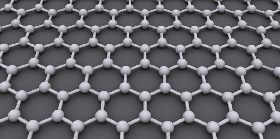
The typical two-dimensional hexagonal structure of graphene. For actual graphene, this honeycomb structure consists of carbon atoms – but now, it can also be recreated using micrometer-size polystyrene particles. Image Credit: Wikimedia Commons
However, many features of the material and its cousins remain unknown, owing to the difficulty of seeing the atoms that make them up. A team of academics from the University of Amsterdam and New York University has finally discovered a surprising solution to this problem.
Recent years have seen a lot of interest in two-dimensional materials consisting of a single, atomically thin layer. Their peculiar characteristics, which set them apart from their three-dimensional “bulk” counterparts, are mostly to blame for this well-deserved attention.
Numerous two-dimensional materials are currently the subject of significant laboratory investigation, with graphene serving as the most well-known illustration.
Unexpectedly, these materials’ unique features depend heavily on their flaws or areas where the crystal structure is imperfect. There, the layer of atoms’ organized arrangement is disturbed, and local atom coordination changes.
Visualizing Atoms
Even though it has been demonstrated that defects are essential for a material’s qualities and that they are frequently either present or intentionally introduced, little is understood about how defects originate and change over time. Atoms are just too small and move too quickly to be directly followed.
The UvA-Institute of Physics and New York University research team developed micrometer-scale models of atomic graphene in an effort to make the imperfections in graphene-like materials visible. They employed so-called “patchy particles” to do this.
These particles interact with the same coordination as atoms in graphene and form the same structure. They are large enough to be seen in a microscope yet tiny enough to imitate many of the characteristics of actual atoms.
The researchers created a model system and utilized it to gain insight into defects, how they develop, and how they change over time. This week, Nature Communications published the findings.
Building Graphene
Each carbon atom in graphene has three neighbors, which are organized in the familiar “honeycomb” pattern. The unusual mechanical and electrical characteristics of graphene are a result of this peculiar structure.
The researchers employed tiny polystyrene particles coated with three much smaller patches of a material, known as 3-(trimethoxysilyl)propyl, or TPM for short, to generate the same structure in their model.
The arrangement of the TPM patches resembled how carbon atoms coordinate in the graphene lattice. Then, in a similar fashion to how the carbon atoms in graphene interact with one another, the researchers made the patches appealing enough that the particles could establish bonds with one another.
When examined under a microscope after being left alone for a few hours, the “mock carbon” particles did, in fact, arrange themselves into a honeycomb lattice. The flaws in the model graphene lattice were subsequently given closer inspection by the researchers.
They noted that the model was successful in this regard as well, exhibiting distinctive defect patterns that are also familiar from atomic graphene.
In contrast to actual graphene, the direct observation and lengthy development period of the model now allows the physicists to monitor these flaws from the very beginning of their production up till the integration into the lattice.
Unexpected Results
New information regarding these two-dimensional structures was discovered as soon as a new perspective on the creation of graphene-like materials was obtained. Unexpectedly, the researchers discovered that the most prevalent type of defect already arises in the initial phases of development when the lattice is not yet constituted.
The lattice mismatch is subsequently “repaired” by another defect, creating a stable defect configuration that either persists or only very slowly heals to a more ideal lattice.
As a result, the model system not only makes it possible to recreate the graphene lattice on a bigger scale for a variety of applications, but direct observations also provide information on the atomic dynamics in this class of materials.
These direct findings in model systems aid in the further engineering of the atomic counterparts since defects are essential to the characteristics of all atomically thin materials, such as for use in ultra-lightweight materials and optical and electronic devices.
Journal Reference
Swinkels, P. J. M., et al. (2023) Visualizing defect dynamics by assembling the colloidal graphene lattice. Nature Communications. doi:10.1038/s41467-023-37222-4.