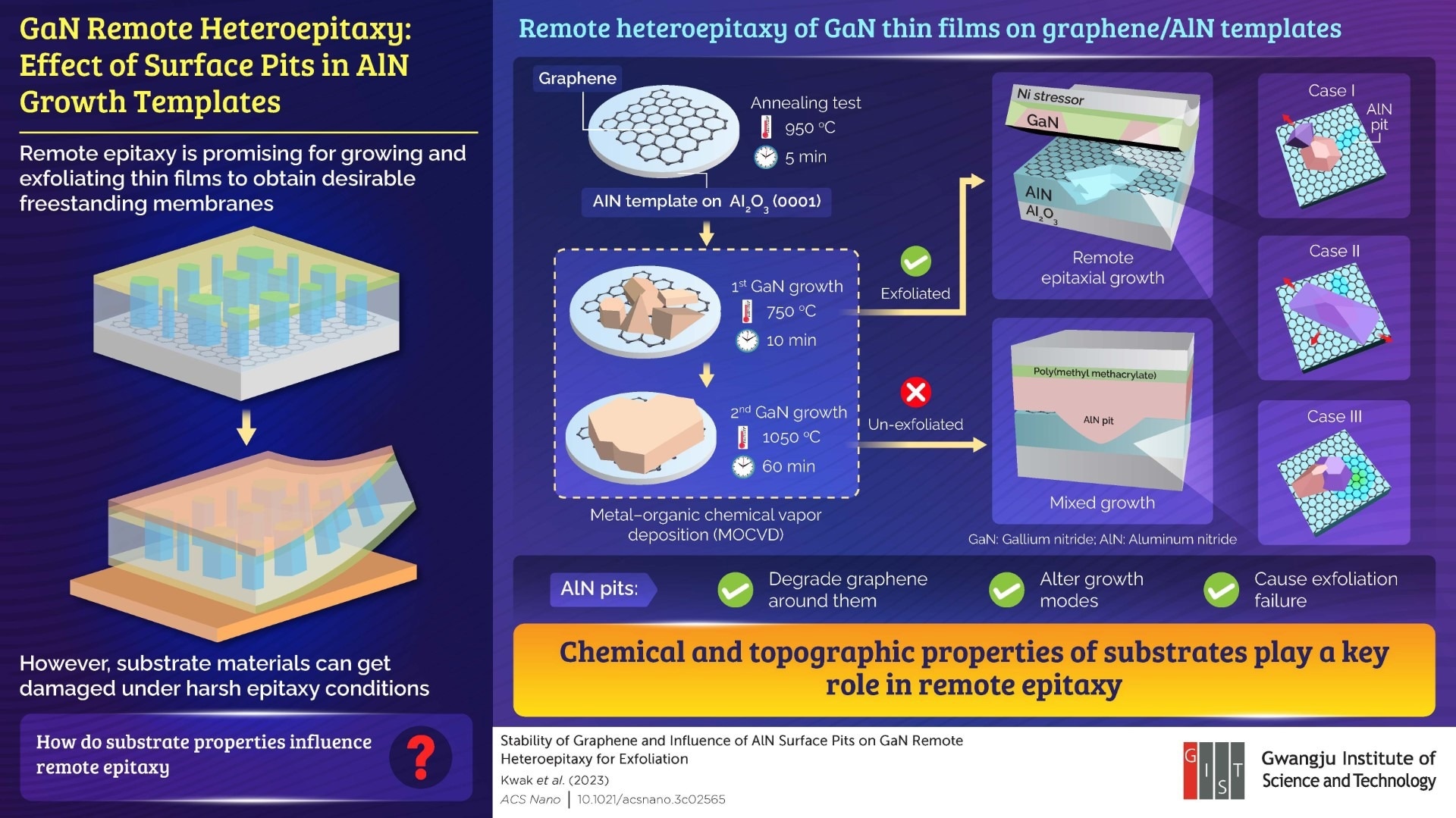
Remote epitaxy, a promising technology for thin film growth and exfoliation, suffers from substrate damage under harsh conditions. In this regard, researchers recently investigated the effect of nano-sized pits on AlN template surface on GaN remote epitaxy. While GaN thin film could be exfoliated at 750 °C, it failed at 1050 °C. At higher temperatures, the nano pits damaged the graphene layer between the template and the film, causing alterations in the film growth mode.

Image Credit: Remote epitaxy
Remote epitaxy has been gaining attention in the field of semiconductor manufacturing for growing thin films that copy the crystal structure of the template, which can later be exfoliated to form freestanding membranes. However, harsh epitaxy conditions can often cause damage to the template materials, such as in the case of remote epitaxy of GaN thin films, promising materials for light-emitting diodes, photodetectors, and power electronic devices, on graphene/AlN templates.
GaN remote heteroepitaxy has not been achieved by a standard metal–organic chemical vapor deposition (MOCVD) technique due to the high temperatures involved in the process. It has been reported that graphene placed on a substrate in an extreme environment such as high temperature or use of an active gas in MOCVD gets damaged due to chemical instability, which causes failure to exfoliate grown GaN films.
Against this background, a team of researchers led by Dong-Seon Lee, Head of the Department of Semiconductor Engineering and Professor at the School of Electrical Engineering and Computer Science at the Gwangju Institute of Science and Technology, has recently used remote epitaxy to grow GaN thin films on graphene/AlN templates by MOCVD and investigated the effect of surface pits in AlN on the growth and exfoliation of these thin films. Their paper was made available online on 6 June 2023 and published in Volume 17, Issue 12 of the journal ACS Nano on 27 June 2023.
The researchers first performed an annealing test at 950 °C for 5 minutes to check the thermal stability of graphene on AlN. Based on its results, they developed a two-step process to grow GaN thin films on the template by MOCVD. The first GaN growth took place at 750 °C for 10 minutes, following which the second growth was performed at 1050 °C for 60 minutes. The exfoliation of the thus-grown GaN thin films was used as a proof of success of the remote epitaxy process. While the films grown at 750 °C could be exfoliated successfully, the separation failed after the second step growth.
Upon deeper analysis, the team found that the nano-sized pits on AlN surface led to the degradation of graphene near them at higher temperatures, which altered the growth modes of GaN thin films. As a result, GaN directly bonded with the AlN substrate, causing the failure of film exfoliation. “Through this study, we revealed for the first time that structural problems in the substrate can also cause peeling failure. These results exemplify the importance of chemical and topographic properties of templates for successful remote epitaxy,” highlights Prof. Lee.
This study provides the primary experimental data that supports the stable implementation of the development of remote epitaxy. When asked about the implications of the present work, Prof. Lee says: “In the near future, GaN remote epitaxy implementation is expected to provide high-quality GaN semiconductors required for the electric vehicle industry. Since substrate recycling is possible, it is expected to change the big picture of the existing semiconductor industry. Further, it will be possible to overcome Moore’s law.”