Comptek Solutions, a leader in advanced passivation technology for the semiconductor industry, proudly announces the successful design and installation of its pilot line, funded by the European Innovation Council (EIC). This state-of-the-art pilot line integrates Comptek's proprietary Kontrox™ passivation technology with other widely used industry techniques such as Atomic Layer Deposition (ALD), delivering a proven, scalable solution for industrial manufacturing specifically targeting power electronics and optoelectronic applications.
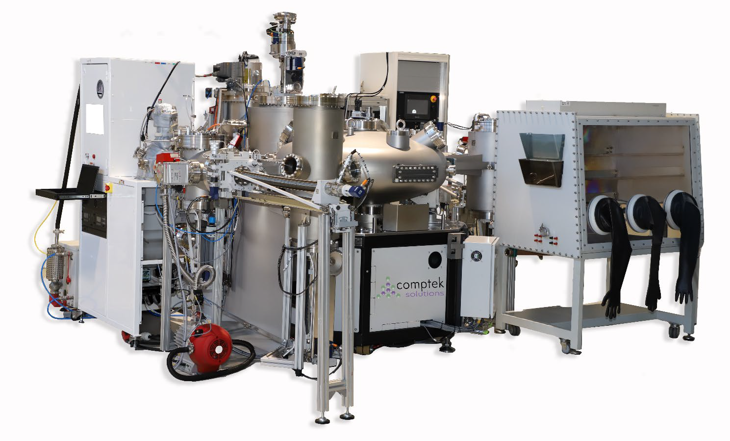
Image Credit: Comptek Solutions
The completion of this pilot line marks a significant milestone for Comptek Solutions in providing revolutionary passivation innovations, enabling a leap in performance and manufacturability for next-generation compound semiconductors. Designed to validate Comptek's innovative Kontrox passivation technology on up to 200mm substrates, this cutting-edge cluster tool integrates the Kontrox passivation process with industry-standard methods, featuring a plasma-enhanced ALD (PE ALD) module, along with advanced functionalities for wet etching and chemical processing in a controlled inert gas atmosphere. With continuous processing that maintains vacuum between different process steps, the system offers tremendous flexibility in developing complex passivation solutions that meet even the most demanding requirements, ensuring superior chip performance and long-term reliability for high-performance semiconductor applications.
"The pilot line we've developed through the EIC-funded 'Enlight' project is a testament to our commitment to pushing the boundaries of passivation technology," said Vicente Calvo Alonso, CEO and Co-Founder of Comptek Solutions. "The possibility to combine our unique Kontrox passivation technique with advanced ALD capabilities allows us to deliver highly customizable and optimized solutions, designed to overcome the challenges and fulfill the needs of power electronics and optoelectronic manufacturers. With this pilot line, we are excited to offer our customers the opportunity to tailor the processes to their exact production requirements, helping them achieve unprecedented performance for their device applications."
A standout feature of this pilot line is the integration of Comptek's Kontrox™ process with ALD technology, implemented using Veeco's PE-ALD FIJI 200 system. This innovative combination provides a transformative approach to minimizing surface defects and creating an exceptionally sharp III-V dielectric interface. The result is superior interface quality, crucial for maximizing chip performance and optimizing yields in a wide range of semiconductor applications, from sidewall passivation layers for µLEDs to complex gate stack dielectrics for power transistors.
The success of this groundbreaking two-year project owes much to the support of the European Innovation Council (EIC). Through the EIC Accelerator funding, the Comptek Solutions team were able to refine its core processes and validate its passivation technology for large-scale industrial manufacturing.
Vicente highlighted the EIC's vital role, stating: "We are deeply grateful to the European Innovation Council for their unwavering support, which has been instrumental in transforming our vision into a reality. The EIC's funding and guidance have enabled us to build a turnkey passivation solution for larger substrates, allowing Comptek Solutions to advance the applicability of our technology to the industrial scale. This achievement would not have been possible without the EIC's belief in the potential of our innovations and their commitment to driving technological breakthroughs in Europe."
The value of compound semiconductor substrates is projected to grow at 17% annually from 2023 to 2029, reaching US$3.3 billion, driven by increasing demand from industries such as automotive, communications, and consumer electronics, with growth in power electronics fuelling the transition to larger substrates like 200mm wafers for SiC and GaN-on-silicon. Meanwhile, the rising use of 150mm InP in datacom and 200mm GaAs and sapphire in microLED displays is driving further demand for advanced semiconductor technologies (Source: Yole Group link). These trends underscore the need for high-quality passivation to ensure optimal performance and reliability in power and optoelectronic applications while promoting sustainable semiconductor manufacturing.
Comptek Solutions' EIC-funded pilot line, with its immense potential for next-level compound semiconductor-based substrate passivation, has already attracted significant interest. Several major manufacturers have already scheduled trial runs to explore its top-tier capabilities for their specialized production needs, and the company's capacity for 2025 is already fully booked. By offering a leading-edge, full-stack passivation solution, Comptek Solutions is uniquely positioned to drive innovation in the evolving semiconductor landscape, helping manufacturers achieve superior efficiency and performance in next-generation and more-than-Moore semiconductor devices.