Image Credit: Nagoya University
Surfaces are essential to many chemical processes, such as corrosion and catalysis. Chemists and engineers must comprehend the atomic structure of a functional material's surface.
“Surface reconstruction” is a phenomenon in which the atoms on the surface are arranged differently than those inside certain materials. This requires surface-sensitive methods to examine, particularly at the atomic level.
Scanning electron microscopy (SEM) has long been a valuable tool for studying nanoscale structures. SEM works by collecting SEs released from a sample’s surface when it is scanned with a focused electron beam. However, it is difficult to observe processes like surface reconstruction, as SEs are typically emitted from a small depth below the surface, especially when only a single atomic layer is involved.
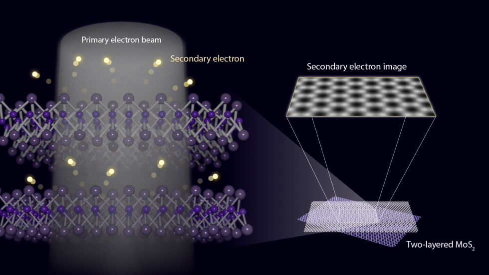
To quantify the amount of information that SE imaging can extract from the surface and subsurface layers, the Nagoya University research team used the most straightforward system possible, a two-layered molybdenum disulfide (MoS2) sample. They used the technique to separate the surface layer from the second layer by stacking two layers of MoS₂.
With a very high surface sensitivity, the researchers discovered that atomic resolution SE imaging works well for detecting surface atomic configurations. Their findings strongly confirmed the method's sensitivity, showing that the intensity of SE pictures from the surface layer was roughly three times higher than those from the second layer.
A single-layer MoS₂ sample's atomic-resolution SE pictures showed beautiful honeycomb-like formations made of sulfur and molybdenum atoms. In addition to being aesthetically pleasing, SE imaging showed overlapping patterns that indicated different atomic configurations in the second and surface layers.
Most notably, the SE yield from the surface layer was about three times greater than from the second layer. This result suggests that the surface layer absorbs or scatters SEs from the second layer. This absorption contributes to the method’s depth sensitivity.
Koh Saitoh, Study Lead Author and Researcher, Institute of Materials and Systems Sustainability, Nagoya University
The group aims to use atomic-resolution SE imaging to uncover the atomic-level surface structure, including surface reconstruction and other distinct surface-formed features. Comprehending these processes is crucial to regulating the development, production, and mechanical and electrical characteristics of nanomaterials.
Journal Reference:
Saitoh, K., et al. (2024) Surface sensitivity of atomic resolution secondary electron imaging. Microscopy. doi.org/10.1093/jmicro/dfae041.