Numerous measurement modes have been advanced to characterize mechanical, magnetic, electrical and thermal properties since Atomic Force Microscopy (AFM) was first developed [1].
Kelvin Probe Force Microscopy (KPFM) [2] is one such prominent mode that facilitates the inspection of the characteristics of both surface morphology and surface potential distribution on a nanometer scale.
KPFM has been widely used to monitor the localized charge distributions on a surface layer [3], surface potential distributions [4] variations in surface work functions [5] and ferroelectric domains [6], across an extensive range of research fields.
By administering AC and DC voltage, KPFM can provide surface topographical information and surface potential/work functions of the sample simultaneously.
KPFM monitors the surface potential and work function of samples by applying a DC bias (VDC) to invalidate tip-sample potential difference, utilizing the same arrangement as Electrostatic Force Microscopy (EFM). The VDC, moderated by the KPFM feedback, is equal to the surface potential (VS) and consequently produces the surface potential map.
In the traditional method, amplitude modulation (AM) KPFM, the measurement signal relates directly to the electrostatic force between sample surface and tip through the amplitude of the AC frequency signal (Figure 1a). This suggests that AM KPFM is greatly affected by the whole AFM cantilever, which reduces the resolution and sensitivity because of an averaging effect [7] [8].
In terms of the spatial resolution and sensitivity of the surface potential measurement, Sideband KPFM has a competitive edge in contrast to AM-KPFM [9].
The AC voltage (VAC) applied between the sample and AFM tip produces an oscillation in both the electrostatic force and its gradient. This oscillation produces a modulation of the resonance frequency of the cantilever (f0).
Sidebands appear at f0 + fAC and f0 – fAC caused by the oscillating force gradient in the frequency spectrum of the cantilever deflection (Figure 1b). The electrostatic force is offset by the application of a DC voltage, which corresponds to the potential difference between the AFM tip and the sample, and the sideband vanishes.
By measuring the DC voltage necessary to offset the electrostatic force, images of the surface potential distribution of the sample can be captured. In addition, the work function distribution can be added, if the work function of the tip is known.
Contrary to AM-KPFM, the Sideband KPFM signal relies on the electrostatic force gradient and is primarily affected by the AFM tip apex. The dependence on the force gradient leads to an enhancement in spatial resolution and potential sensitivity.
Throughout this study, the results obtained with AM-KPFM and Sideband KPFM on well-defined samples with extended areas of different surface potentials are presented. From these results, a direct comparison of the spatial resolution of AM-KPFM and Sideband KPFM under equivalent conditions is carried out.

Figure 1. Frequency spectra for AM-KPFM (a) and Sideband KPFM (b). Image Credit: Park Systems Corp
Materials and Methods
Sideband KPFM
To measure electrical properties of a sample surface, Sideband KPFM is an elective AFM mode. Figure 2 exhibits the connection diagram of Sideband KPFM, which utilizes two lock-in amplifiers to measure the amplitude and phase of each sideband.
On lock-in amplifiers 2 and 3, a signal holding a frequency of f0 ± fAC is used as the reference signal (produced by lock-in amplifier 2) to decouple the sideband signals with a frequency of f0 ± fAC in the deflection signal (identified by lock-in amplifiers 2 and 3).
To alter the DC voltage, the decoupled signals from the two lock-in amplifiers are averaged and utilized for the feedback. The AFM controller applies an equivalent VDC so the averaged sideband peak size becomes zero (as tip bias servo in Park SmartScan).

Figure 2. Connection diagram of Sideband KPFM. Image Credit: Park Systems Corp
Test Samples and AFM Cantilever
ZYH grade highly-ordered pyrolytic graphite (HOPG, SPI Supplies) was used for highlighting layer-by-layer surface potential differences. A silicone substrate with low conductivity polymer dots was utilized to exhibit the surface potential difference of two separate materials.
An IFX dopant calibration sample (NP20, Infineon) was selected to observe the stepwise electrical signal. This sample was made up of 5 various n-type implant areas so that the electrical signals could be compared.
All imaging was conducted with the use of an Au coated NSC36-C (resonance frequency, 65 kHz; spring constant, 0.6 N/m; length, 130 μm) with identical AFM parameters.
Results and Discussion
Three separate samples are analyzed in this study so that the electrical resolution performances of AM-KPFM and Sideband KPFM can be sufficiently compared.
The surface potential images of HOPG by AM-KPFM and Sideband KPFM are illustrated in Figure 3. Sideband KPFM verifies the strong contrast due to the HOPG layer, whereas AM-KPFM shows blurred edges.
Sideband KPFM has around double the higher surface potential difference on layers (~70 mV) than AM-KPFM (~35 mV, red arrow), as displayed in the line profile analysis. It also exhibits mini HOPG fragments quite clearly, while AM-KPFM shows a blurred image.

Figure 3. The comparison of surface potential between AM-KPFM (a) and Sideband KPFM (b) on a HOPG sample with a line profile analysis (c). Image Credit: Park Systems Corp
Subsequently, the analysis of polymer dots on a silicone substrate was conducted by AM-KPFM and Sideband KPFM. In addition, a comparison of Sideband KPFM both in and out of lift mode was carried out to study the non-contact feedback capabilities for Sideband KPFM.
In Figure 4, all images display comparative points between the polymer dots and the silicone substrate. Yet, AM-KPFM demonstrates a lower surface potential contrast than Sideband KPFM with lift mode. The difference between the no-lift mode and a 5 nm lift mode does not vary significantly for Sideband KPFM, which is confirmed in the line profile analysis.
Between the polymer dots and the silicone substrate, surface potential differences are somewhere around 180 mV in AM-KPFM, ~300 mV for the no-lift Sideband KPFM and ~330 mV for the 5 nm lift Sideband KPFM.
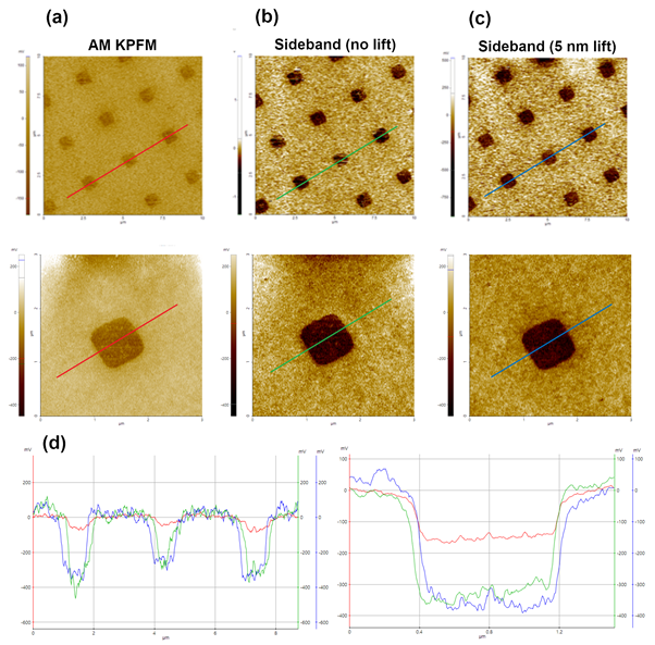
Figure 4. Comparison of surface potential between AM-KPFM (a), Sideband KPFM with no lift (b) and Sideband KPFM with 5 nm lift (c) on polymer dots sample with line profile analysis (d). Image Credit: Park Systems Corp
Finally, to compare stepwise electrical resolution, AM-KPFM and Sideband KPFM were used on a IFX dopant calibration sample. In AM-KPFM, varying doping level of n-type implant are acknowledged; yet, measurement of the steps in the electrical signal was complicated.
In comparison, the stepwise electrical signal is clearly exhibited in both no-lift and 5 nm lift Sideband KPFM. Predicated on numerous repetitive tests, all Sideband KPFM analyses demonstrate enhanced spatial resolution and potential sensitivity than those of AM-KPFM.
Sideband KPFM can monitor step-by-step surface potential differences, while AM-KPFM only picks-up an incremental signal decrease, as indicated by the line profile.

Figure 5. Multiple measurements on AM-KPFM (a), Sideband KPFM with no lift (b) and Sideband KPFM with 5 nm lift (c) on an IFX dopant calibration sample with line profile analysis (d). Image Credit: Park Systems Corp
Conclusions
This study concludes, by way of contrast between AM-KPFM and Sideband KPFM using a variety of samples, that Sideband KPFM has better spatial resolution and potential sensitivity when compared to AM-KPFM.
In surface potential images, Sideband KPFM demonstrates a clear electrical contrast and discovers any minor potential changes that may be relative. From line profile analysis, it was discovered that the surface potential differences measured by Sideband KPFM are greater than that of AM-KPFM, emphasizing the enhanced performance of Sideband KPFM.
In all samples tested, there is no variance shown in the contrast between no lift and 5 nm lift in Sideband KPFM.
Topography mapping is carried out in True Non-Contact Mode without tapping between AFM tip and sample surface, because of the precise nature of Park Systems’ AFM feedback system. It is therefore possible to acquire the true surface morphology and a clean KPFM signal without crosstalk.
Since the advances of KPFM, it has become one of the better AFM options used in semiconductor engineering and by surface material science. It is an exceptional method for surface potential or work function uniquely mapping on the nanoscale, and the Sideband KPFM option provides enhanced spatial resolution and greater electrical sensitivity for material characterizations.
References
1. Quate, C. F., Gerber, C., & Binnig, C. (1986). Atomic force microscope. Phys. Rev. Lett, 56(9), 930-933.
2. Nonnenmacher, M., O’Boyle, M. P., & Wickramasinghe, H. K. (1991). Kelvin probe force microscopy. Applied physics letters, 58(25), 2921-2923.
3. Lü, J., Delamarche, E., Eng, L., Bennewitz, R., Meyer, E., & Güntherodt, H. J. (1999). Kelvin probe force microscopy on surfaces: investigation of the surface potential of self-assembled monolayers on gold. Langmuir, 15(23), 8184-8188.
4. Liu, L., & Li, G. (2010). Electrical characterization of single-walled carbon nanotubes in organic solar cells by Kelvin probe force microscopy. Applied Physics Letters, 96(8), 33.
5. Bieletzki, M., Hynninen, T., Soini, T. M., Pivetta, M., Henry, C. R., Foster, A. S., ... & Heiz, U. (2010). Topography and work function measurements of thin MgO (001) films on Ag (001) by nc-AFM and KPFM. Physical Chemistry Chemical Physics, 12(13), 3203-3209.
6. Wu, W., Horibe, Y., Lee, N., Cheong, S. W., & Guest, J. R. (2012). Conduction of topologically protected charged ferroelectric domain walls. Physical review letters, 108(7), 077203.
7. Melitz, W., Shen, J., Kummel, A. C., & Lee, S. (2011). Kelvin probe force microscopy and its application. Surface science reports, 66(1), 1-27.
8. Garrett, J. L., & Munday, J. N. (2016). Fast, high-resolution surface potential measurements in air with heterodyne Kelvin probe force microscopy. Nanotechnology, 27(24), 245705.
9. Stan, G. (2020). High-speed digitization of the amplitude and frequency in open-loop sideband frequency-modulation Kelvin probe force microscopy. Nanotechnology.

This information has been sourced, reviewed and adapted from materials provided by Park Systems.
For more information on this source, please visit Park Systems.