Due to its application in a variety of fields, ranging from electronics to biomedical technologies, nanotechnology is attracting greater attention within the scientific community [1].
Progress in many of the technology’s applications relies primarily on the capacity to manufacture nanostructured materials such as polymers and semiconductors, among others [2, 3].
Numerous methods have been established for the manufacture of nanostructures; the more commonplace ones are electron beam lithography and focused ion beam lithography.
However, these methods can be both complicated and expensive to operate. To get past such problems, atomic force microscopy (AFM) nanolithography is a powerful method that has been developed [1-3].
This technique is relatively straightforward and inexpensive [2]. AFM nanolithography is separated into two general groups predicated on their mechanistic and operational principles; bias-assisted and force-assisted AFM lithography [2].
In the bias-assisted technique, a bias voltage is applied to the tip to produce an oxide pattern on the metallic or semiconductor substrate [4, 5]. In contrast, the force-assisted method applies a greater force to the tip to produce fine grooves on the surface of polymer-like samples.
This is achieved by mechanically scratching, pushing, or pulling the surface atoms and molecules with a sharp tip; the interaction between the tip and the sample is primarily mechanical [2, 3].
This technical note details the capability of AFM nanolithography to produce nanopatterns by using Park NX10 Atomic Force Microscope. The tip bias mode is utilized to generate oxide patterns on the silicon substrate.
Successful pattern fabrication is established by Lateral Force Microscopy (LFM). The inclusion of lithography and LFM mode with AFM allows it to fabricate nanopatterns and acquire both topography and frictional data synchronously. The results acquired in this experiment verifies that the fabricated oxide nanopatterns are executed successfully.
Experimental
To draw nanopatterns onto a silicon substrate, a Park NX10 AFM was utilized for AFM nanolithography.
LFM imaging was performed after the lithography process to verify the successful fabrication of the oxide patterns on the surface as well as to establish any difference between the surfaces of the oxide layers and silicon substrate. During the experiment, a PPP-CONTSCPt cantilever with a nominal spring constant (k = 0.2 N/m) and resonance frequency (f = 25 kHz) was used.
Results and Discussion
Bias-Assisted AFM Nanolithography
Bias-Assisted AFM Nanolithography is a method best-explained as material modification (oxidation) via the application of voltage bias to the AFM tip. The applied bias on the tip leads to the production of an electric field between the tip and the sample.
The field ionizes water molecules created between the tip and the sample, which results in local anodic oxidation (LAO) used to manufacture surface nanoscale oxide features.
The tip acts as a nanoscale electrode for current injection or collection throughout the lithography process [1, 2]. The amount of oxide layer that forms on the surface is dependent on the extent of the bias and humidity applied.
The thickness of a pre-designed nanoscale oxide pattern of device structure increased due to the increment of applied tip voltages as described in the previous study [2].
Thus, it was determined that the tip voltage affected the amount of oxide formed on the surface. Accordingly, a schematic illustration of bias-assisted AFM nanolithography is exhibited in Figure 1.
![Schematic illustration of Bias-Assisted AFM Nanolithography [4, 5].](https://d1otjdv2bf0507.cloudfront.net/images/Article_Images/ImageForArticle_5634_1611208885733452.png)
Figure 1. Schematic illustration of Bias-Assisted AFM Nanolithography [4, 5]. Image Credit: Park Systems
Throughout this study, Park lithography software was utilized to develop and apply nanolithography to the surface of the sample: a silicon substrate was used as a sample.
The application of –10 V led to an increased electric field around the tip, which resulted in the cleavage of water molecules into ions H+, OH- and O- ions [5]. The OH- and O- ions are then driven away from the biased tip and form SiO2 after reacting with the silicon.
On the surface of the silicon substrate, the nanoscale oxide pattern forms along the scan area of the lithography scan.
Lateral Force Microscopy
The vertical deflection and the torsion of the cantilever are recorded and used to obtain the topography and surface frictional characteristics of the sample in the Lateral Force Microscopy (LFM) mode.
The cantilever movement in both the vertical direction and the torsion is followed through a position sensitive photo detector (PSPD) that is made up of four domains (a quad-cell), as displayed in Figure 2. Surface topographical information and frictional information are acquired by using Equations 1 and 2.
Equation 1: Topographic information = (A+C) - (B+D)
Equation 2: Frictional information = (A+B) - (C+D)
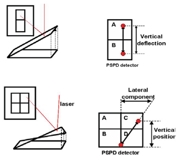
Figure 2. Schematic illustration of laser position on PSPD in the operation of AFM (top) and LFM (bottom). Image Credit: Park Systems
Figure 3 exhibits the topography, frictional data and equivalent line profile of the images subsequent to the lithography process. The images were captured by employing the LFM mode.
Both topography and frictional data can be acquired simultaneously since LFM is a contact mode, thus enabling correlation between topographic and frictional properties.
The AFM topography image (Figure 3b) indicates that the design has a diameter of approximately 17 µm and is a Christmas ball pattern composed of numerous micro-structures with heights ranging from 0.2–1.5 nm. Figure 3e portrays the line profiles that were produced using the Park XEI software to offer a more direct signal comparison.
By analyzing the line profiles acquired with the LFM forward (green line) and backward (blue line) scans, insight into the frictional characteristics of the sample are obtained. The LFM signal shifts upward in the forward scan, suggesting that the movement of the cantilever was impeded as a result of a change in frictional force as the tip bypassed the oxide layer.
On the contrary, the LFM signal moved downward during the backward scan, which, again, was a consequence of the cantilever being dragged by the surface due to the larger frictional interaction between the cantilever and the surface.
Consequently, it can be determined that the frictional coefficient of the oxide layer is greater than that of the silicon substrate.
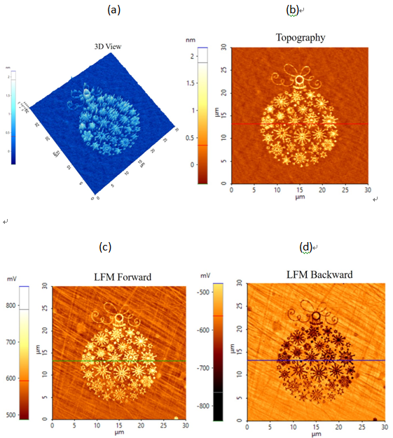

Image Credit: Park Systems
Conclusion
Thus, it was determined that the use of AFM nanolithography produces nanoscale oxide patterns in a silicon substrate by utilizing the Park NX10 system. The voltage bias-mode method was utilized in the AFM nanolithography process.
The application of –10 V voltage bias on the tip resulted in the successful manufacturing of the nanoscale oxide features on the surface. The LFM mode was also performed and the results established the successful manufacture of the oxide patterns.
The AFM nanolithography, as outlined in this study, is, therefore, a useful technique for the fabrication of next-generation materials and devices with inherent nanoscale features.
References
- A. Pimpin, et al., Review on Micro- and Nanolithography Techniques and their Applications.Engineering Journal.
- S. Hutagalung, et al., Nanoscale Patterning by AFM Lithography and its Application on the Fabrication of Silicon Nanowire Devices. Sains Malaysiana 43(2), (2014): 267–272.
- R. Garcia, et al., Advanced scanning probe lithography. Nature Nanotechnology 9, 577–587 (2014); doi:10.1038/nnano.2014.157
- J. Voves, Nanoelectronics and nanolithography. https://www.researchgate.net/publication/228859246_Nanoelectronics_and_nanolithography
- A. Bernal et al., LOCAL ANODIC OXIDATION ON SILICON (100) SUBSTRATES USING ATOMIC FORCE MICROSCOPY. http://www.scielo.org.co/pdf/dyna/v79n174/v79n174a08.pdf

This information has been sourced, reviewed and adapted from materials provided by Park Systems.
For more information on this source, please visit Park Systems.