Scanning Capacitance Microscopy (SCM) and Scanning Spreading Resistance Microscopy (SSRM) are both well-established scanning probe-based techniques for two-dimensional carrier profiling.
Driven by the microelectronics industry seeking 2D alternatives for their 1D carrier/dopant profiling methods, such as Capacitance-Voltage (C-V) measurements, Scanning Resistance Profiling (SRP) and Secondary Ion Mass Spectrometry (SIMS), these methods were developed early.
In SSRM, while scanning the probe, the resistance of the current passing through the nanoscale tip-sample contact is measured. The key to its increased spatial resolution and sensitivity is embedded in the presence of a pressure induced metallic pocket underneath the tip apex, which almost leads to an ohmic tip sample contact.
The measured resistance is consequently controlled by the spreading resistance and therefore relies on the local sample resistivity ρ:
Rspreading = ρ/4a
Where a indicates the contact size, exceptionally high spatial resolution (~ 1 nm) and increases in sensitivity and dynamic range (1014-1020 cm-3) are the principal benefits of SSRM.
Using a high frequency capacitance sensor while scanning the probe in SCM, small capacitance variations (~10-21 F) between the tip and the sample are measured.
Highly doped regions demonstrate low differential capacitance dC/dV, while less doped areas show a relatively larger capacitance alteration. The primary benefits are the large dynamic range and the carrier type sensitivity as n- and p-type show opposing phases in their dC/dV signals.
It is difficult to convert the measured values directly into quantitative values for carriers across each method because of a lack of comprehensive information available on the probe and sample surface.
To convert resistance/differential capacitance to resistivity/carrier concentrations, a calibration against a known standard, therefore, tends to be the most straightforward method.
In fact, both techniques demonstrate advantages and disadvantages but can be quite complementary; SSRM offers the highest spatial resolution while SCM gives carrier type sensitivity.
As current innovations in advanced devices are entering the sub 10 nm nodes, the demands on materials and device characterization are being pushed to their limits. Every aspect of the measurement requires optimization for successful measurements, for example, the probe, the sample preparation and the measurement environment.
This application note reviews the performance of the Park NX-Hivac atomic force microscope (AFM) from Park Systems [1] for SSRM and SCM applications, based on the following three samples:
- A p-type doped silicon calibration sample (imec CS08-SiB): a sample comprised of different Boron doped epitaxial silicon layers (~600 nm) with known doping concentration (Figure 1).
- An n-type doped silicon calibration sample (imec CS01-SiAs): a sample made up of a variety of arsenic doped epitaxial silicon layers with known doping concentration (Figure 5). Additionally, this sample possesses a p-type doped layer embedded in the stack.
- Buried oxide sample: a 0.5 nm oxide layer sandwiched in between a highly doped Si and a poly Si layer (Figure 2).
These samples are recorded on the Park NX-Hivac AFM system, operational in vacuum conditions (~5e-5 mbar) using imec Full Diamond probes [2].
SSRM – Basic Performance
To calculate the repeatability of SSRM measurements, the p-type calibration sample is first measured. It is evident in Figure 1 that exceptional repeatability is accomplished in SSRM measurements on silicon. The repeatability is improved in the highly doped layers.
As a reference, for identical scanning parameters, it is typical that repeatability of 15-20% is reached in air. This highlights the added value of high vacuum [3].

Figure 1. SSRM measurement on a p-type doped silicon calibration sample performed in vacuum. The coloured resistance cross-sections are taken from single line scans and the black line is the average over those 5 scan lines. The repeatability is plotted in purple (right Y-axis). Image Credit: Park Systems
The buried oxide sample is subsequently measured to evaluate the resolution of SSRM. Figure 2 highlights that the 0.5 nm oxide layer embedded in silicon can be simply observed in SSRM measurements as an increase in the resistance.

Figure 2. High resolution SSRM measurement on a 0.5 nm oxide layer sandwiched in between highly doped Si and poly Si layers. The resistance cross-section is taken from a single scan line. Image Credit: Park Systems
The doubling of the resistance on the thin oxide demonstrates that the electrical contact radius is similar to that of the oxide thickness, emphasizing a sub-nm resolution [2].
To confirm the benefits of conducting SSRM measurements in a vacuum environment, the p-type calibration sample is finally recorded in air and in vacuum with the same probe. An overview of the results is displayed in Figure3.
As anticipated, in order to capture an image of similar quality, the required force applied to the tip for an appropriate electrical tip-sample contact had to be enhanced by almost 50% when transferring the experiment to an ambient environment from a vacuum.
This observation is indicative of the fact that the metallic pocket below the tip apex is induced at a lower pressure in vacuum in comparison to that of ambient air.
Measurements in a vacuum environment can therefore be conducted with a reduced force applied to the tip, which will extend the lifetime of the tip with less wear and thus higher resolution [2].

Figure 3. SSRM measurements on a p-type doped silicon calibration sample performed in vacuum and in air with the same probe. The resistance cross-sections are the average over 50 scan lines. Image Credit: Park Systems
From the results displayed above, it can be determined that the repeatability and resolution of SSRM measurements carried out on the Park NX-Hivac AFM are state-of-the-art and that the vacuum conditions in the chamber are advantageous for conducting repeatable SSRM experiments.
SSRM – Device Measurements & Calibration
The calibration samples ordinarily enable the conversion of the resistance map of an unknown sample to a carrier concentration map. The same probe is therefore utilized for the calibration sample and scan parameters as with the measurement on the sample of interest.
Figure 4, for instance, displays the resistance and carrier concentration maps of an n-type doped silicon layer in a solar cell.

Figure 4. SSRM resistance and carrier concentration maps of an n-type doped silicon layer in a solar cell sample. Image Credit: Park Systems
The carrier concentration map derives from the resistance map by utilizing the calibration curve that is displayed in Figure 5. Measuring over the five layers with known doping levels enables the resistance data points to be taken from the average resistance values. The calibration curve is generated by interpolation of these data points.

Figure 5. SSRM measurement on an n-type doped silicon calibration sample. The resistance cross-section is taken from the average of 50 scan lines. The resistance versus dopants data points are taken from the average resistance values measured over the 5 layers with known doping levels in the calibration sample. Image Credit: Park Systems
It can be determined that the good measurement repeatability on both the sample and the standard enables the precise resolution of the active carrier concentration in a sample with unknown carrier levels.
SCM
To assess the performance of SCM on the Park NX-Hivac AFM, the n-type doped silicon calibration sample is used. Next to the n-type epitaxial layers, this sample also has a p-type doped layer in between the substrate and the n-layers.
Respectively, Figure 6 displays the dC/dV amplitude and the dC/dV phase map received from an SCM measurement on the n-type calibration sample. The n and p-layers are clearly identifiable from the phase map.

Figure 6. SCM dC/dV amplitude and phase measurements on ann-type doped silicon calibration sample. The dC/dVamplitude cross-sectionis taken from the average of 50 scan lines. Image Credit: Park Systems
The various n-type layers with varying doping concentrations also show a clear contrast in the dC/dV amplitude map. These results indicate the carrier type sensing capability of SCM and the carrier concentration sensitivity, despite the spatial resolution not equalling that of SSRM.
Besides Si, another captivating application of SCM is on III-V material stacks. Figure 7 shows the results of an SCM measurement on a doped InGaAs stack. These results indicate the ability to extract information about the carrier concentration and the carrier type.
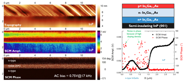
Figure 7. SCM measurement on a doped InGaAs stack. The dC/dV amplitude and phase cross-sections are taken from the average of 100 scan lines. Image Credit: Park Systems
Conclusions
This study demonstrates how scanning spreading resistance microscopy (SSRM) and scanning capacitance microscopy (SCM) can take up the challenges of carrier profiling that cutting edge devices entering the sub 10 nm nodes possess, given access to the right microscopy tool.
This study identified that Park NX-Hivac is an influential tool meeting the challenges of ever-shrinking devices due to its application of electrical SPM modes, including SSRM and SCM, in a high vacuum environment.
In addition, it is concluded that the use of Park NX-Hivac vacuum results in a considerable noise reduction leading to an average repeatability of 6.1% for SSRM measurements.
References
- Park NX-Hivac, Retrieved from https://www.parksystems.com/en/products/research-afm/specialized-afm/nx-hivac
- Hantschel, T., et al. Diamond scanning probes with sub-nanometer resolution for advanced nanoelectronics device characterization, Microelectronic Engineering 159, 46-50 (2016).
- Eyben, P. et al. Fundamentals of Picoscience, Subnanometer Characterization of Nanoelectronic devices. Edited by Sattler, K.D., CRC Press (2014)

This information has been sourced, reviewed and adapted from materials provided by Park Systems.
For more information on this source, please visit Park Systems.