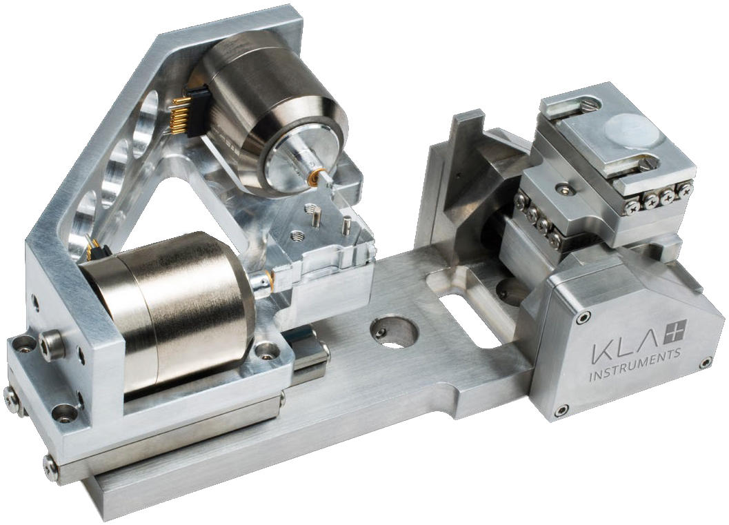
Experience the unbounded freedom a NanoFlip nanoindentation instrument offers your materials research lab. The NanoFlip is a nanoindentation instrument that provides limitless freedom in a materials research laboratory. This instrument is an essential tool for advanced materials mechanical testing because it has the ability to eliminate all environmental constraints and provide steady reliable data for highly challenging experiments.
The trademark of NanoFlip’s proprietary flip design is the high performance versatility, because of which the instrument is able to deliver remarkable results both during in situ testing and ambient testing. Irrespective of the presence of vacuum, the NanoFlip can provide equally superior results.
This instrument can also be used when frequent transitions with widespread sample control are required and when imaging integration is needed.
The NanoFlip is designed with Piezo stage technology in a compact 3-axis system. It can be mounted on most vacuum chambers or even under various imaging systems. Sample targeting before mechanical testing and viewing the sample after the test are facilitated by a fourth rotating axis that moves the sample in 90°.
All of the tools inside a vacuum chamber can be used fully, due to the 90° sample manipulation. The NanoFlip helps in sample preparation, targeting, and mechanical testing. A complete evaluation of the sample without leaving the vacuum environment is also possible.

Image Credit: KLA Instruments™
Key Features
The main features of the NanoFlip are given below:
- Scratch Option - Available scratch option features maximum scratch distance of 2.5 mm, maximum normal load of 50 mN, and a maximum scratch speed of 500 µm/s
- Method Packs - The available method packs consist of methods, tips and standards for biomaterials, thin films and polymers
- Automated Tip Calibration - Unique tip-calibration system that is incorporated into the software helps in accurate, fast, and automated tip calibration
- Precise Targeting - Sample stage movement of 25 mm in the Z-axis, 21 mm in the X-axis, and 21 mm in the Y-axis with 1 nm resolution allows precise sample targeting over a wide area
- Data Confidence - Instruments from KLA offer highly reliable and widest range data in the industry, with the capacity for dynamic excitation frequencies from 0.1 Hz to 1 kHz
- Excellent Specifications - With a time constant of 20 µs, the NanoFlip is the only nanoindenter in the market to simultaneously match specifications for a noise floor of <0.1 nm, maximum indenter travel of 50 µm, a digital resolution of 0.02 nm and drift rates <0.05 nm/s
- Decouple Force and Displacement - Electromagnetic actuators are used in all systems produced by KLA Instruments; they are linear devices that intrinsically decouple force and displacement, providing a resolution of 3 nN, a maximum force of 50 mN, and an ultra-low noise floor of <200 nN
- Limitless Imaging Options - When experiments are conducted ex situ, the NanoFlip can work under any imaging system including optical microscopes, AFMs and optical profilometers, providing virtually infinite imaging options
- Vacuum Compatible - The NanoFlip is suitable for in situ environments such as FIBs, SEMs, and vacuum chambers as it is designed to be fully vacuum compatible and has a unique sample flipping capability
- Seamless Transitions - Revolutionary Fib2Test Technology enables users to tilt the sample 90° to seamlessly changeover from FIB to indentation test within a dual beam SEM without having to remove the sample
- 3D and 4D Mapping - 3D and 4D mapping of materials is performed by the optional NanoBlitz 3D topography and NanoBlitz 4D tomography software
- Load-Frame Stiffness - The NanoFlip delivers a load-frame stiffness of over 1,000,000 N/m
Customer Testimonials
As an active user of various nanoindentation systems over the past 19 years, I am happy to report that we are extremely pleased with all of our recent acquisitions from KLA. Our lab is currently equipped with the iNano, InSEM HT and NanoFlip. Among the non-technical standout features are the instrument's ease of installation and the excellent efficiency of NMI's remote internet support. All three systems were completely self-installed in just a few hours or less. With their small footprint and integrated components that require very few electrical connections, the systems are lightweight and easy to move around.
Erik G. Herbert Ph.D., Materials Science and Engineering, University of Tennessee