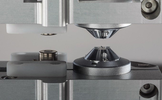
The Filmetrics® R54-Series is the new sheet resistivity mapping tool from KLA Instruments™. It has been developed for automated mapping of 200 mm and 300 mm semiconductor and compound semiconductor wafers, and can be configured with either four-point probe (4PP) or non-contact eddy current (EC) measurement capability.
The R54 has been improved for quantifying ion doping and implant characterization, light-sensitive implant and epi wafers, resistivity measurement, and non-contact metal film thickness uniformity.
Normally, the R54 system configuration is chosen depending on the wafer size and intended application. The R54-4PP configuration is suggested for ion implant and thin metal film processes while the R54-EC configuration is perfect for quantifying thicker metal layers, sensitive surfaces, and buried conductive films. Both come in 200 mm and 300 mm versions to house bigger samples.
Listed below are the usual samples mapped by the R54:
- Metal films, foils, and coatings
- Conductive polymers
- Solar cell and flat panel display (FPD) layers
- Epitaxial wafers
- Ion implants
- Semiconductors, dielectric substrates, and compound semiconductors
The R54 hardware platform shares the Filmetrics F54 software interface and enclosure design, with the Filmetrics RsMapper software which is specialized for resistivity measurements.
The main features of the R54 include:
- Sheet resistance measurement spans 10 orders of magnitude on semi-conductive and conductive films
- High precision automated X-Y-θ stage offers complete wafer travel up to 300 mm
- I-V curve plotting and current ramp scans
- Windows software interface with simple recipe setup
- Coarse and precision height control and surface approach
- User-specified sample point mapping for rectangular, polar, linear, and custom configurations for high-density linear scans and uniformity mapping

The R54-200 four-point probe (4PP) as it approaches the surface of an unpatterned wafer. Image Credit: KLA Instruments™