The Park NX10 provides consistent data that can be replicated and published at the highest nano resolution. It features the world’s true non-contact AFM that increases tip life while prolonging the sample and flexure based independent XY and Z scanner for unparalleled accuracy and resolution.
Technical Information
Accurate AFM Solutions for General Research
Tall Sample 1.5 µm Step Height
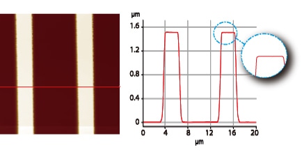
- Scan Mode: Non-contact mode, Topography from Z position sensor
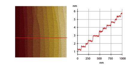
Hard Sample Tungsten film

- Scan Mode: Non-contact mode, Topography from Z position sensor
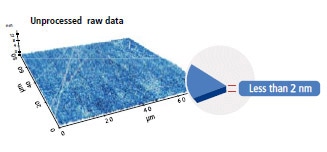
Flat Sample Atomic Steps of Sapphire Wafer
- 0.3 nm step height, Scan Mode: Non-contact mode, Topography from Z position sensor
Soft Sample Collagen Fibril
- Scan Mode: Non-contact mode, Topography from Z position sensor
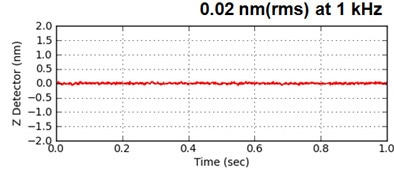
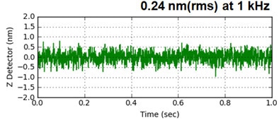
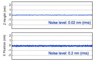
Accurate AFM Measurement with Low Noise Z Detector
Low Noise Z Detector of Park NX10 AFM
- Used as the default topography signal
- Noise level is the lowest in the industry, unmatched by any other
- Key technological advance and design feature of NX platform
Park NX Series
The noise level of the Z position detectors of the Park NX
Park XE Series
The noise level of the Z position detectors of the Park XE
The Z detector is considered to be the key technological advance of the new NX-series AFM. This is a new type of strain gauge sensor innovated by Park. At 0.2 Angstrom, it is the best Z-detector noise in the industry. The noise level is low enough so that the Z-detector can be used as the default topography signal. The difference can be highlighted if the new NX-series AFM is compared with the earlier generation of Park’s AFM model, XE. Observing the atomic steps on sapphire wafer becomes difficult if the Z-detector noise is too high. The noise level of the height signal from the Z detector of the Park NX AFM is identical to that of the Z-voltage-based topography.

The topography images of a sapphire wafer obtained from NX10
The topography images of a sapphire wafer obtained from XE-100
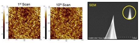
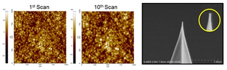
Accurate AFM Scan by True Non-Contact™ Mode
True Non-Contact™ Mode

- Immunity from parameter dependent results
- Less tip wear = Prolonged high-resolution scan
- Non-destructive tip-sample interaction = Minimized sample modification
Tapping Imaging
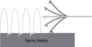
- Highly parameter-dependent
- Quick tip wear = Blurred low-resolution scan
- Destructive tip-sample interaction = Sample damage and modification
The Best User Convenience by Design
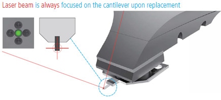
Easy Tip and Sample Exchange
The unique head design allows effortless side access enabling users to effortlessly snap new tips and samples into place by hand. The cantilever is ready for scanning without the requirement for any tricky laser beam alignment by using pre-aligned cantilevers mounted on to the cantilever tip holder.

Lightning Fast Automatic Tip Approach
User intervention is not needed for Park’s automatic tip to sample approach and the tip also engages in just 10 seconds after loading the cantilever. By monitoring the cantilever response to the approaching surface, Park NX10 is capable of initiating an automatic fast tip to sample approach within 10 seconds of cantilever loading. Low noise signal processing by the NX electronics controller and rapid feedback by the high speed Z scanner enable quick engagement to the sample surface without any user intervention. It just works with minimal user involvement.
Easy, Intuitive Laser Beam Alignment
With the improved pre-aligned cantilever holder, the laser beam is focused on the cantilever upon placement. Users can effortlessly find the laser spot with the help of the natural on-axis top-down view, considered to be the only one in the industry. It is possible to intuitively move the laser spot along the X- and Y-axis by rotating its two positioning knobs since the laser beam falls vertically on the cantilever. This results in allowing the user to effortlessly find the laser and position it on PSPD using Park’s beam alignment user interface. All that is needed after this point is a minor adjustment in order to maximize the signal to start collecting the data.
Key Features

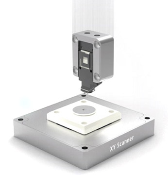
1. 2D Flexure-Guided Scanner with 50 µm and 50 µm Scan Range
The XY scanner consists of symmetrical 2D flexure and high-force piezoelectric stacks provides high orthogonal movement with minimal out-of-plane motion and also high responsiveness vital for precise sample scanning in the nanometer scale.
2. High Speed Z Scanner with 15 µm Scan Range

Guided by a flexure structure and driven by a high-force piezoelectric stack, the standard Z scanner has a Z-servo speed of more than 48 mm/sec tip velocity, and a high resonant frequency of more than 9 kHz (typically 10.5 kHz) which enables accurate feedback. It is possible to extend the maximum Z scan range from 15µm to 30µm with the optional long scan range Z scanner.
3. Low Noise Position Sensors
The applied Z voltage is replaced as the Topography signal by the industry leading low noise Z detector. In addition, the low noise XY closed loop scan minimizes the backward and forward scan gap to be less than 0.15% of the scan range.
4. Motorized XY Sample Stage
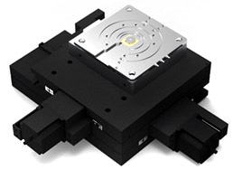
XY Sample Stage is motorized to make it easy for navigating and positioning the sample to the region of interest. This motorized stage has a resolution of 0.6 um (using micro-stepping) on both axis.
5. Step-and-Scan Automation
Step-and-Scan enables user-programmable multiple region imaging by using the motorized sample stage. The Step-and-Scan process consists of:
1) Scan an image
2) Lift the cantilever
3) Move the motorized stage to a user defined coordinate
4) Approach
5) Repeat the scan
This automated feature brings about an increase in productivity by minimizing user assistance during repetitive imaging processes.

6. Accessible Sample Holder
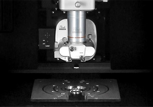
The unique head design allows for an open side access to sample and tip. The maximum sample size one can place on the stage is either 150 mm diameter x 20 mm or 200 mm diameter x 20 mm based on the travel range option chosen for the XY sample stage.
7. Expansion Slot for Advanced SPM Modes and Options
Enhanced SPM modes are enabled by simply plugging an option module to the expansion slot. Option compatibility throughout the product line is allowed by the modular design of the NX-series AFM.
8. Direct On-Axis High Powered Optics with Integrated LED Illumination

Custom designed objective lens with ultra long working distance (51 mm, 0.21 NA, 1.0 µm resolution) allows optical view with unprecedented clarity. The intuitive direct on-axis sample view from the top permits users to navigate the sample surface effortlessly to find the target area. For a higher vision resolution the EL20x objective lens of Long Travel Head is used, which has 20 mm working distance, 0.42 NA and 0.7 µm resolution. The enlarged sensor size of the CCD provides wide field of view of the sample without compromising the optics resolution. The software-controlled LED light source provides ample illumination onto the sample surface for clear sample observation.
9. Auto Engage by Slide-to-Connect SLD Head
The AFM head is easily removed or inserted by sliding it along a dovetail rail. This automatically locks the head into its pre-aligned position and connects it to the control electronics with a positioning repeatability of a few microns. The low coherency of the Super Luminescence Diode (SLD) enables accurate imaging of highly reflective surfaces and precise measurements for pico-Newton Force-distance spectroscopy. The SLD wavelength eliminates interference issues for users interested in integrating the AFM with experiments in the visible spectrum.
10. Vertically Aligned Motorized Z Stage and Focus Stage
The motorized focus stage and the motorized Z stage both make it possible of engaging the cantilever to the sample surface while constantly maintaining a clear vision for the user. Since the focus stage is motorized and software controlled, it has the precision essential for liquid cell applications and transparent samples.
High Speed 24-bit Digital Electronics
All NX-series AFMs are controlled and processed by the same NX electronics controller. The controller is an all digital, 24-bit high speed electronics unit, which insures the accuracy and speed of Park’s True Non-Contact ModeTM for speed and accuracy. With its low noise design and high speed processing unit, the controller is perfect for nanoscale imaging and precise voltage and current measurements. The embedded digital signal processing capability adds to the economics and functionality of Park’s AFM solutions for advanced researchers.
24-bit Signal Resolution for XY and Z Detectors
- 0.001 nm resolution in Z (15 µm Z)
- 0.003 nm resolution in XY (50 µm XY)
Embedded Digital Signal Processing Capability
- Spring constant calibration (thermal method)
- 3 channels of flexible digital lock-ins
- Digital Q control included
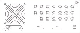
Intergrated Signal Access Ports
- 7 inputs and 3 outputs
- Dedicated and programmable signal input/output ports