EV Group (EVG), a leading supplier of wafer bonding and lithography equipment for the MEMS, nanotechnology and semiconductor markets, today announced that the Fraunhofer Institute for Silicon Technology (ISIT) has purchased an EVG®850TB/DB fully automated bonding/debonding equipment solution. The system has been shipped and installed at Fraunhofer ISIT's facility in Itzehoe, Germany, where it is being used in the development and production of next-generation power devices, including PowerMOS and Insulated Gate Bipolar Transistors (IGBTs).
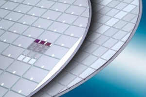
 Insulated Gate Bipolar Transistor (IGBT) wafer processed on EVG(r)850TB/DB fully automated bonding/debonding system. (PRNewsFoto/EV Group)
"We've collaborated with EV Group for several years in developing thin-wafer handling processes for power devices due to their extensive expertise in temporary bonding and debonding," stated Dr. Wolfgang Windbracke, deputy director, Fraunhofer ISIT. "The commitment and support that their process development team has provided—as well as access to EV Group's cleanrooms, demo tools and applications labs—has been very helpful in our development efforts. With EV Group's automated temporary bonding and debonding system now installed at our development facility, we can further accelerate our research and development efforts and ramp up manufacturing of our newest generation of power devices faster at the joint-production facility in Itzehoe that we share with Vishay Semiconductor."
Power devices are microelectronic components that are essential functional elements in electrical equipment such as voltage converters, power amplifiers and switch-mode power supplies. Thinning power device wafers enables the devices that are produced to have lower electrical resistance, which reduces power loss and enhances product performance. Temporarily bonding device wafers to carrier wafers helps ensure the integrity of the device wafers during the wafer thinning process. Since even the smallest thickness variations of the final device can have a critical impact on performance, process reliability and uniformity are important characteristics in wafer handling and bonding/debonding to ensure safe processing and optimal yields. Today, EVG's temporary bonding/debonding tools are the most advanced in the world with the highest bond accuracy and unprecedented thickness uniformity results.
"We're very pleased to be able to count Fraunhofer ISIT as a customer as well as a development partner on thin-wafer applications for advanced power device development and production," stated Paul Lindner, executive technology director, EV Group. "With more than 10 years of experience in temporary bonding/debonding and with the largest installed base of tools in volume production, EV Group is the clear leader in the temporary bonding/debonding market. Customers and development partners alike leverage our leading process development team expertise and cleanroom facility to support their advanced process development efforts, as well as our cutting-edge process equipment to help take them to the next level and enable them to ramp up their next-generation processes into production."
The EVG850TB/DB automated system is a highly flexible tool that can be configured to support a variety of bonding materials. The system is used to temporarily bond a device wafer to a rigid carrier wafer for safe and efficient processing of the device wafer. After subsequent power device processing (back thinning, etching, implantation, lithography, metallization, annealing, etc.), the device wafer is debonded from the carrier substrate using various techniques dependent of the intermediate material. The EVG850TB/DB features a special robot end-effector handling solution and a cassette station for thin-wafer output providing customers with the highest flexibility available in a modular configuration. These special features enable the system to fit any specialized customer process.
About Fraunhofer ISIT
Fraunhofer ISIT in Itzehoe is one of Europe's most modern research facilities for microelectronics and microsystems technology. The heart of the institute is the 3,000 m2 cleanroom, big enough to operate not only research projects but also to produce the developed microchips on industrial scale. ISIT develops in close cooperation with industrial partners in power electronic components and microsystems. These miniaturized components are used in power conversion, in the environment, and traffic engineering, communication technology, automotive industry, mechanical engineering and medical applications.
The IC-Technology department is focussed on microelectronic components. Advanced power semiconductor devices are developed from the design phase to prototyping, including simulation and electrical characterisation. In the field of active devices the ISIT is concentrating on IGBTs, PowerMOS transistors and diodes. The Insulated Gate Bipolar Transistor (IGBT) is the most important power semiconductor device in the medium power range with voltages >400 V. To improve their performance with respect to robustness, switching and conduction losses, ISIT is focussing on the development of ultrathin Fieldstop IGBTs.
Dedicated expertise lies on new device architectures, e.g. charge compensations devices, and monolithic integration of power devices. Moreover, advanced fabrication techniques such as ultrathin wafer technology and laser annealing is available.
About EV Group (EVG)
EV Group (EVG) is a leading supplier of equipment and process solutions for the manufacture of semiconductors, microelectromechanical systems (MEMS), compound semiconductors, power devices and nanotechnology devices. Key products include wafer bonding, thin-wafer processing, lithography/nanoimprint lithography (NIL) and metrology equipment, as well as photoresist coaters, cleaners and inspection systems. Founded in 1980, EV Group services and supports an elaborate network of global customers and partners all over the world.