Image Credit: Tokyo Institute of Technology.
Eradicating the etching procedure by directly manufacturing nanowires onto the silicon substrate might result in a significant breakthrough in spintronic device fabrication. Unfortunately, when directly fabricated nanowires are annealed, the inherent stresses in the wire cause them to change into droplets.
A group of scientists headed by Professor Yutaka Majima of the Tokyo Institute of Technology has discovered a solution to the problem. The researchers described a new fabrication method for producing L10-ordered CoPt nanowires on silicon/silicon dioxide (Si/SiO2) substrates. The study was published in the journal Nanoscale Advances.
Our nanostructure-induced ordering method allows the direct fabrication of ultrafine L10-ordered CoPt nanowires with the narrow widths of 30nm scale required for spintronics. This fabrication method could further be applied to other L10-ordered ferromagnetic materials such as iron–platinum and iron–palladium compounds.
Yutaka Majima, Professor, Tokyo Institute of Technology
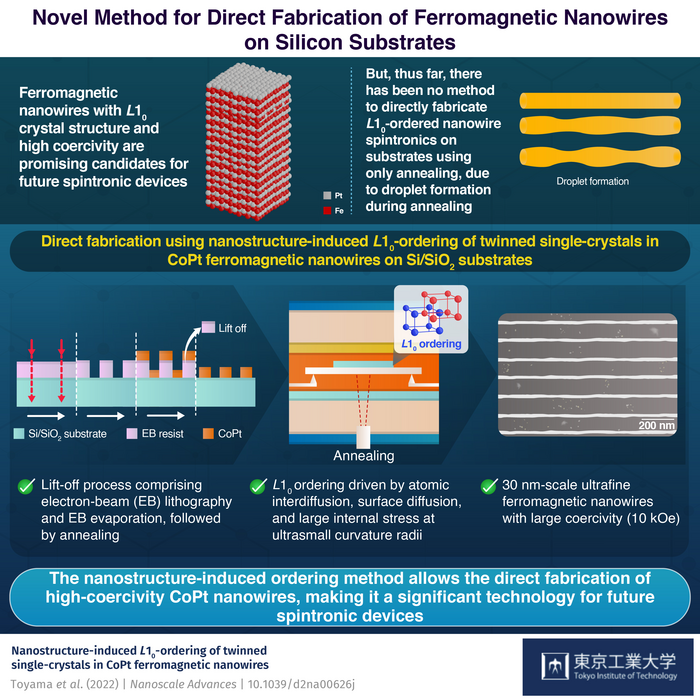
In this work, the investigators first coated a Si/SiO2 substrate with a substance called a “resist” and exposed it to electron beam lithography and evaporation to form a stencil for the nanowires.
The substrate was then covered with a multilayer of CoPt. The deposited samples were then “lifted off,” leaving CoPt nanowires behind, and the nanowires were then annealed at high temperatures. The team also used various characterization techniques to evaluate the produced nanowires.
Researchers discovered that the nanowires acquired L10-ordering throughout the annealing procedure. This transition was caused by atomic interdiffusion, surface diffusion, and exceptionally high internal stress at the nanowires’ ultrasmall curvature radii of 10 nm. They also discovered that the nanowires have a high coercivity of 10 kiloOersteds (kOe).
The internal stresses on the nanostructure here induce the L10-ordering. This is a different mechanism than in previous studies. We are hopeful that this discovery will open up a new field of research called ‘nanostructure-induced materials science and engineering.’
Yutaka Majima, Professor, Tokyo Institute of Technology
The breakthrough fabrication technique’s broad applicability and ease of use will undoubtedly make a substantial contribution to the field of spintronics research.
Journal Reference
Toyama, R., et al. (2022) Nanostructure-induced L10-ordering of twinned single-crystals in CoPt ferromagnetic nanowires. Nanoscale Advances. doi.org/10.1039/D2NA00626J.