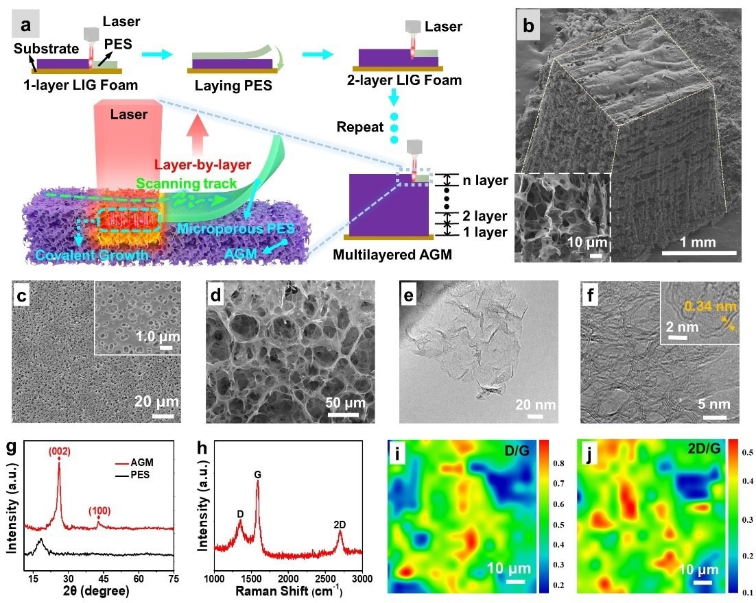
Researchers from the Chinese Academy of Sciences’ Hefei Institutes of Physical Science (HFIPS) have presented a laser-assisted layer-by-layer covalent growth approach for producing highly crystalline all-graphene macrostructures (AGMs).
 Layer-by-layer covalent growth and the characterization of AGMs. Image Credit: LI Nian
Advanced Functional Materials published the findings.
Graphene is a two-dimensional carbon material with remarkable mechanical, electrical, thermal, and optical characteristics. To enable large-scale applications, graphene must be effectively prepared and assembled at the macroscopic level.
Traditional approaches, such as liquid phase self-assembly, 3D printing, and catalytic template procedures, can only create non-covalent weak connections between graphene sheets, resulting in crystal structure discontinuities. This constraint impairs the electrical characteristics of graphene macrostructures.
A covalently linked AGM with micro-to-macro scaling electrical characteristics was created in this study by laminating a microporous polyethersulfone (PES) membrane. Using a laser, each stack layer of PES membrane was entirely carbonized, and smooth inter-layer boding was accomplished in an air environment.
The researchers discovered the covalent growth mechanism of AGM using molecular dynamics modeling. This method provided a 100-fold improvement in cross-layer conductivity over non-covalent construction.
AGMs have been shown to be successful in a variety of settings, including supercapacitor electrodes. In addition to energy storage, the covalent growth approach for AGMs is fundamentally important for other industries as well, including electronics, electromagnetic shielding, and sensors, where effective and superior techniques for producing macroscopic graphene are crucial.
Journal Reference:
Song, Y., et al. (2023) Macro-Sized All-Graphene 3D Structures via Layer-by-Layer Covalent Growth for Micro-to-Macro Inheritable Electrical Performances. Advanced Functional Materials. doi:10.1002/adfm.202305191