EUV Tech (EUVT), a global leader in manufacturing at-wavelength EUV metrology equipment, is excited to announce the next generation of EUV zoneplate microscopy. The AIRES® (Actinic Image REview System) microscope captures and characterizes photomask defects, supporting both EUV scanner emulation mode as well as a variety of enhanced imaging modes that facilitate defect classification.
The distinguishing feature of the AIRES microscope is its patented low-aberration zoneplate imaging system. Zoneplates are ultra-compact, high-wavefront quality diffractive optics. Using this zoneplate technology, AIRES produces an ultra-high magnification image of the photomask with a significantly smaller physical footprint than possible with alternative solutions.
The highly flexible AIRES microscope supports a large number of illumination modes to match typical scanner conditions and further integrates multiple complementary imaging modes through automated zoneplate exchange capabilities.
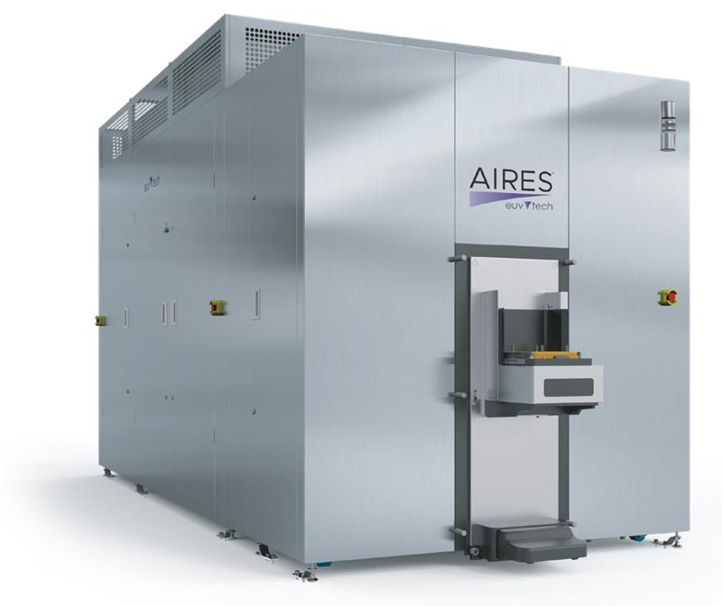
Image Credit: EUVTech
“The enhanced AIRES microscope represents an unprecedented combination of imaging power and flexibility enabling both highly accurate defect printability measurements, as well as unique defect classification capabilities previously only possible on synchrotron-based tools,” explained Patrick Naulleau, CEO of EUV Tech.
The ability to obtain detailed defect information makes it possible for photomask manufacturers to make targeted mask repairs without expensive print checks. And due to its simplified, compact design, AIRES has a significantly lower cost of ownership relative to similar EUV microscopy tools. As a highly performant metrology solution, AIRES enables the semiconductor industry to continue to produce smaller and more powerful chips while maintaining high-quality and efficient production. Looking ahead at the next leap in EUV lithography, EUV Tech’s patented zoneplate microscopy provides the flexibility to rapidly switch to high-NA imaging.
The release of this latest-generation AIRES tool marks a culmination of years of development to future-proof photomask and wafer manufacturing to meet the escalating demands of the semiconductor industry and AI technology.