For photovoltaic (PV) power generation to provide a considerable amount of the global energy needs, it is imperative that the price of panels, for every Watt generated, is reduced. Thin film inorganic compounds such as CdTe and Cu(In, Ga) Se2(CIGS) are the best prospects for low-cost, high volume photovoltaic power generation.
Currently, the two aforementioned materials constitute nearly 20% of solar panel sales, with the possibility that this fraction will progressively increase, because of the following advantages over Si:
- The direct band gap of these materials implies that a significantly reduced thickness of material, 2–5 µm, was required compared to Si, 100–400 µm.
- This reduced thickness results in considerably lowered requirements for crystalline quality in the solar absorber; it paves the way for a wider variety of possible production routes, increasing throughput and lowering costs.
Advantages of Attolight System
Compared with other techniques, cathodoluminescence provides characterization of these thin film PV materials with unparalleled spatial resolution. In particular, the Attolight system offers the following advantages:
- Defects such as grain boundaries and dislocations can be analyzed with respect to their signal intensity as well as their CL spectroscopic profile. This can give information about both the electrical activity of the defects and any chemical segregation effects.
- The cooling stage is highly stable and enables high-resolution scans down to 10 K, providing information about the spatial distribution of dopants and defects levels. Besides, the temperature dependence of excited states can be determined, providing activation energies for these states.
- The local measurement of CL emission lifetimes provides unparalleled characterization of composition gradients and defects; carrier lifetimes are a significant factor in PV where they must diffuse to the contacts so as to be collected.
This combination of data regarding the energy levels, structure, and defects in photovoltaic materials provides a detailed analysis.

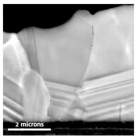
SEM image of a CdTe/CdS photovoltaic heterojunction in cross-section.

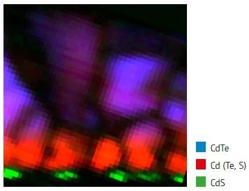
CL map of the same cross-section color-coded by emission frequency. The interdiffusion of sulfur at the junction is clear in the CL dataset.

This information has been sourced, reviewed and adapted from materials provided by Attolight.
For more information on this source, please visit Attolight.