High manufacturing yield is crucial for photovoltaics (PV) and thin film batteries (TFB) to cost compete against traditional batteries and fossil fuels. Yield loss and lower performance are caused by pin holes in the CdS layer of CdTe/CdS and CdS/CIGS PV devices and the LiPON layer of TFBs. SEM plan view analysis lacks the depth resolution to establish if holes penetrate completely through a layer.
Attolight’s CL Technology
Benefits of Attolight’s CL technology are:
- Reduces development time by allowing pinhole detection for unit processes; enables comparison of how process variables and deposition methods influence pinhole formation
- Evaluates composition gradients and defect density during pinhole detection
- Rapid automated Mapping: 25 µm x 25 µm area mapped in 65 seconds

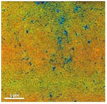
CL identifies pinholes by detecting light from the underlying layer as shown below:

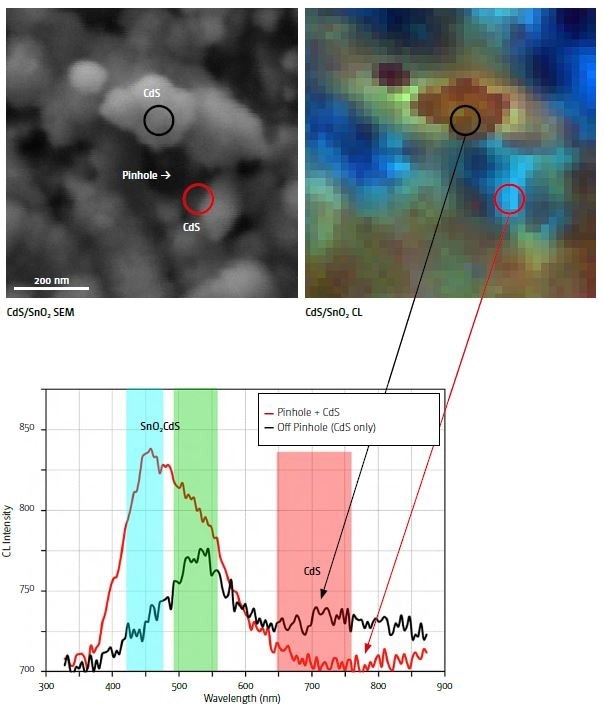
The following SEM image and the CL map show an actual application of this technique to pinholes in CdS deposited by Chemical Bath Deposition on SnO2. The emission lines are:
- CdS (light areas in SEM): red (mid-gap defect states) and green (band gap)
- Pinholes (black areas in SEM): blue (mid-gap defect states) from SnO2 at bottom of holes.
Circles correspond to single CL points. Circle diameter = electron interaction volume (100 nm @ 5 keV).


This information has been sourced, reviewed and adapted from materials provided by Attolight.
For more information on this source, please visit Attolight.