Semiconductor quantum structures emerged in the second half of the 20th century, fueled by promises of far superior performances especially where light emission is concerned. The dimensionality was brought down to point-like quantum dots (QDs). QDs have interesting similarities with atoms, and therefore significant efforts were made to evaluate their properties.
Advantages of Cathodoluminescence Measurements
The growth of quantum dots embedded in filamentary crystals, called nanowires (NWs), became relevant because of the strong interaction between NWs and light.
Specifically, QDs in NWs are predicted to be significant elements in quantum technologies, including cryptography and quantum communications. However, the reduced dimensionality of both NWs (ar. 100-200 nm in diameter) and QDs (ar. 5-10 nm) can make it difficult to measure the QDs properties. Above all, assessing the absolute QDs position and resolution between proximal dots with full-optical measurement is difficult owing to diffraction limitations.
These limitations can be overcome with cathodoluminescence measurements, which help assess the position of QDs and their appearance based on the host NWs’ properties. For Attolight’s structures, made of GaAs and AlGaAs, the Attolight CL-SEM makes it possible to operate at cryogenic temperature, a condition that is vital to observe light emission from the QDs. Compared to the traditional system, the Attolight microscope also offers the following advantages:
- The large numerical aperture guarantees a very high signal-to-noise ratio, resulting in a shorter exposure of the QDs to the electron beam and thus lowering the risk of bleaching and accelerating the experiment.
- Thanks to the higher signal, a spectrometer-CCD detection channel can be easily used, eliminating the need for photomultiplier tube and yielding directly fast hyper-spectral mapping. The wide emission spectral range is subsequently captured (in this case, from 650 nm to 900 nm).
- The spatial resolution helps resolve closely lying dots and local features, for example changes in the matrix crystal phase.
To sum up, analysis performed with the Attolight system easily provides information on both the QDs and the matrix that otherwise cannot be obtained by other methods without tremendous effort and compromises.

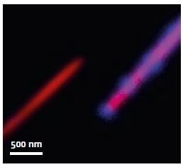
Close-up of two NWs tip. Red now represents the emission from GaAs core (820 nm) of the wire, while blue regions mark th e QDs emission (670 nm). Dots at less than 500 nm can be easily resolved. (Specimen temperature: 10 K)

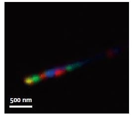
Mapping of the QDs location with respect to the emitted wavelength. Blue, green, and red correspond to 3 wavelengths between 650 and 700 nm. Some dots emit at several wavelength, resulting in composite colors. (eg. Yellow)

This information has been sourced, reviewed and adapted from materials provided by Attolight.
For more information on this source, please visit Attolight.