In this article, 3D polymeric atomic force microscopy (AFM) tips, referred to as 3DTIPs, are introduced. The key differences between standard silicon AFM tips and the new 3DTIPs design will be covered, as well as the impact these new probes will have on nanoscale research.

Image Credit: sanjaya viraj bandara/Shutterstock.com
Atomic Force Microscopy
3DTIPs were developed and presented in 2022 by a team of researchers at New York University Abu Dhabi’s Advanced Microfluidics and Microdevices Laboratory (AMMLab).
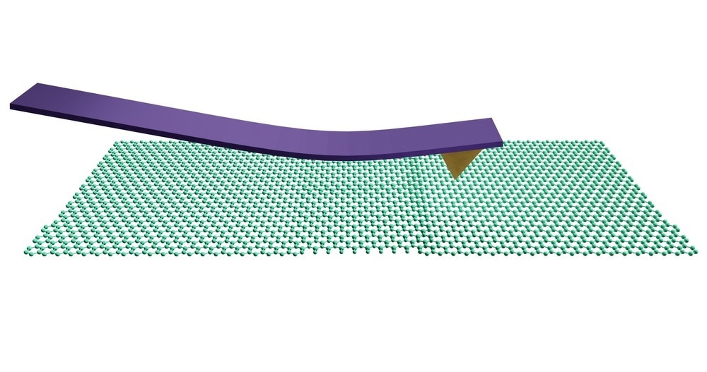
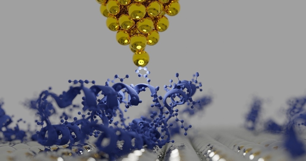
AFM provides a three-dimensional profile of a surface at the nanoscale by measuring the attractive and repulsive forces between the sharp tip of the atomic force microscope and the surface of a sample.
The tip is attached to a cantilever, which in turn, is attached to a mounting base. AFM has provided significant and outstanding discoveries in the fields of nanophysics, solid-state physics, microbiology and medicine, as well as many other fields.
Some key findings from using AFM are the atomic structures of inorganic materials, observing molecular interactions within protein complexes, and time-lapse imaging of RNA replications by a polymerase enzyme.
Comparing Atomic Force Microscopy Tips
There are three key innovative differences between the silicon AFM tips available on the market and the new multipurpose 3DTIPs.
First, 3DTIPs are manufactured from SU-8 resin using the two-photon polymerization technique. This is a fast and highly effective layer-by-layer 3D printing technique of micro- and nanoscale objects, enabling swift, reliable production of 3DTIPs.
Second, 3DTIPs integrate the mounting base, cantilever and tip into one single product, thus allowing individual components to be designed to fit each other perfectly. This has the added advantage of designing and manufacturing an array of 3DTIPs with a constant separation distance between cantilevers.
Third, the new probes make it possible to refine the tip by using one of two methods that enhance the performance and resolution quality: the focused ion beam etching process and integrating carbon nanotubes into the design of the 3DTIPs.
Innovations Following AFM Tip Advancements
The two-photon polymerisation (2PP) technique is extremely flexible with the designs of the new AFM probes. This layer-by-layer printing method can facilitate complex structures that incorporate the tip, cantilever and mounting base with high precision.
The current technique used to create silicon tips is 2D micromachining. This traditional method cannot make as extended a range of tips as the 2PP technique. As such, probes can be modified to suit a much wider range of sample surfaces.
The 2PP technique also allows the added advantage of being able to design and manufacture an array of 3DTIPs with a constant separation distance between cantilevers. Researchers can utilize this to create an array that can be used independently or in parallel for images that must account for surface modifications.
The 2PP technique drastically reduces the production and manufacture time of AFM probes. For well-designed 3DTIPs that incorporate the mounting base and an array of cantilever-mounted tips, printing time can be as low as 15 minutes. Furthermore, the SU-8 resin that the 3DTIPs are made from is very durable. This ensures the tip remains sharper for longer, extending longevity, cost-effectiveness, and consistent image quality.
The team at AMMLab showed that 3DTIPs grant higher-resolution imaging than standard silicon tips, leading to more detailed topographical measurements of a variety of samples.
Scientists may be able to observe previously unknown phenomena of inorganic structures or develop a deeper understanding of time-dependent biological processes. In this way, insight into solid-state physics and quantum mechanics can be gained. Furthermore, researchers can learn to correctly diagnose diseases and create highly effective medicines. The team also showed that 3DTIPs enable high-speed scanning of samples.
Scientists will be able to produce more images in the allotted time for measurements. Increasing the amount of observations ensures the results are rigorous and reproducible, necessary for scientific discovery.

Image Credit: sanjaya viraj bandara/Shutterstock.com
Improving Observations
As alluded to, it is possible to enhance 3DTIPs via the process of focussed ion beam (FIB) etching. 3DTIPs that have been FIB-etched have a smaller tip radius and a higher aspect ratio than silicon AFM tips, providing greater stability in the cantilever. This means images of samples that are soft and easily distorted by the tip, such as biological samples like DNA, have a minimal disturbance.
Another method for improving observations is to integrate carbon nanotubes (CNTs) into the design of 3DTIPs. CNT-integrated probes improve imaging resolution and allow 3DTIPs to perform optimally in both air and liquid environments.
The researchers did, however, discuss in their introductory paper one disadvantage to the 3DTIPs probes. In AFM, the quality factor describes how the energy is dissipated in the cantilever, such that a higher quality factor produces a lower energy dissipation per image.
A higher quality factor is preferred, and a tip with a higher quality factor will contribute towards a better frequency resolution. According to experiments undertaken by the researchers at NYU Abu Dhabi, the typical quality factor of a silicon tip in air is 100-150, but 3DTIPs can obtain a maximum quality factor of 40. The team suggests that more research should be conducted into increasing the quality factor of 3DTIPs, which they have left for future experiments.
Conclusions
To conclude, this article has introduced the new AFM 3DTIPs that researchers from NYU Abu Dhabi’s AMMLab manufactured this year. 3DTIPs make use of the 2PP 3D printing technique to facilitate a range of designs with an integrated tip, cantilever and mounting base.
The new multifunctional AFM probes provide valuable upgrades compared to silicon tips in the form of high-resolution and high-speed imaging in both liquid and air environments. The use of SU-8 resin ensures high durability and extended longevity of probes. All of the improvements listed above combined into a single probe will certainly lead to advancements in nanoscale discoveries. New findings will benefit many different fields of science and industry.
References and Further Reading
Ayoub Glia, Muhammedin Deliorman & Mohammad A. Qasaimeh. (2022) 3D Generation of Multipurpose Atomic Force Microscopy Tips. Advanced Science, p. 2201489 DOI: 10.1002/advs.202201489
New York University (2022) Researchers develop novel 3D atomic force microscopy probes: Advancement paves the way for a range of potential AFM novel applications and nanoscale discoveries. ScienceDaily, 26 July 2022, www.sciencedaily.com/releases/2022/07/220726132514.htm
H. J. Butt, K. H. Downing & P. K. Hansma (1990) Imaging cells with the atomic force microscope. Biophys. J. Vol 105, pg 58, p. 1473, https://doi.org/10.1016/1047-8477(90)90098-W
C Rivetti, M Guthold & C Bustamante, (1999) Wrapping of DNA around the E.coli RNA polymerase open promoter complex. EMBO J, 1999, pp. 4464-75, DOI:https://doi.org/10.1093%2Femboj%2F18.16.4464
T. Strahlendorff, G. L. Dai, D. Bergmann & R. Tutsch (2019) Tip wear and tip breakage inhigh-speed atomic force microscopes. Ultramicroscopy, 201, pp. 28-37, DOI:10.1016/j.ultramic.2019.03.013
N. R. Wilson & J. V. Macpherson (2009) Carbon nanotube tips for atomic force microscopy. Nature Nanotech 4, pp. 483–491. https://doi.org/10.1038/nnano.2009.154
Disclaimer: The views expressed here are those of the author expressed in their private capacity and do not necessarily represent the views of AZoM.com Limited T/A AZoNetwork the owner and operator of this website. This disclaimer forms part of the Terms and conditions of use of this website.