With the EM ACE600 sputter coater, users can confidently prepare the fine-grained thin coatings required for electron microscopy research. Users can increase the number of samples produced with each run due to the accurate, automated carbon and sputter-coating procedures that generate reproducible, reliable results.
With the ease of front door loading, automation, and receipt-based coating processes - initiated at just the push of a button - the EM ACE600 makes routine sample preparation simple, reliable, and time-efficient.
High Vacuum Coating System for a Wide Range of Applications
The EM ACE600 sputter coater is adaptable and has a configurable metal process chamber, making it ideal for various applications.
Users can reach their workflow goals and meet the requirements of their laboratories by running up to two different sources in a single preparation process and can even configure the EM ACE600 for advanced cryo operations.
EM ACE600 carbon, e-beam, and sputter coater with cryo transfer dock. Image Credit: Leica Microsystems-Nanotechnology & EM Sample Preparation-EMEA
The EM ACE600 carbon and sputter coater allows users to:
• Enhance the contrast of nanometer-scale structures such as DNA strands or proteins
• Provide layers of protection for sensitive samples
• Execute high-resolution imaging of non-conductive or flat specimens
• Expand the system for cryo applications
• Produce thin, but strong support layers for TEM grids
Sputter Coating
Reproducible High-Quality Thin Films With Sputter Coating
Users can employ the EM ACE600 high vacuum coating system to consistently produce high-quality, sputter-coated thin films. With the automated, receipt-based sputter coating process, users can create the ideal conditions for advanced coating requirements and achieve consistent results.
Users can perform SEM analysis at high magnifications up to 200 kX and beyond with a base vacuum of <2×10⁻⁶ mbar, and fine-balanced process parameters for various sputter targets. The sample distance and coating angle can also be adjusted to match the needs of the morphology of the sample.
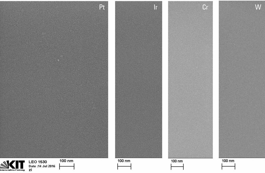
2 nm thick fine-grained sputter coatings of different materials deposited onto SiOx substate, 200 kX magnification. Image Credit: Leica Microsystems-Nanotechnology & EM Sample Preparation-EMEA
Users can employ a Meissner trap to increase the vacuum to 10–7 mbar regime, then experiment with sputter targets or sample materials that are oxygen-sensitive to improve coating results even further.
Carbon Coating
Reproducible, High-Quality Thin Films With Carbon Coating
Users of the EM ACE600 can create high-quality carbon films utilizing e-beam evaporation, carbon thread coating, or carbon rod coating.
Since then, carbon thread evaporation has become a popular method.
The EM ACE600’s unique adaptive pulsing method was developed by Leica Microsystems. It can manufacture robust, amorphous, and precise films with a sub-nanometer thickness while minimizing the heat impact on the sample.
Carbon thread is an excellent option if the user requires thin, strong, clean TEM support layers, large homogenous carbon layers, or diffuse (protection) coatings.
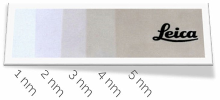
Precise Carbon deposition of 1–5 nm thick carbon films. Image Credit: Leica Microsystems-Nanotechnology & EM Sample Preparation-EMEA
The e-beam evaporator can be used for dedicated applications such as rotary shadowing. Its modest beam divergence is excellent for shadow coating to improve the edge contrast of nanometer-scale structures.
The EM ACE600 Adapts to its User’s Needs
The EM ACE600’s large reconfigurable metal process chamber enables it to run multiple processes in a single coater instrument without breaking the vacuum. Users can employ two sputter sources or a sputter head in tandem with an advanced carbon thread evaporator to enable multi-layer metal coatings during a single preparation process.
Users can:
- Choose from e-beam, strong carbon thread, and sputter coater sources
- Produce evenly distributed thin films over the whole 100 mm stage due to the optimized two-source concept with a rotating stage and two angled ports
- Upgrade their system at any time on site
- Equip their EM ACE600 with glow discharge sputtering
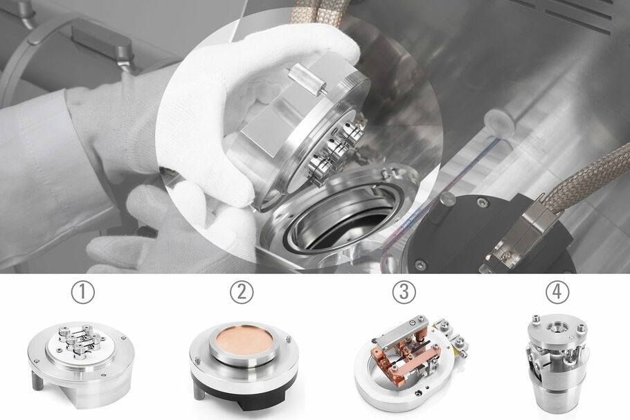
ACE600 configurable ports for two sources. Choose from: 1-carbon thread evaporation | 2-sputtering | 3-carbon rod evaporation | 4-e-beam evaporation. Image Credit: Leica Microsystems-Nanotechnology & EM Sample Preparation-EMEA
Choose the Right Workflow for Experiments
The EM ACE600 helps users obtain high-quality results when conducting biological and material science experiments. Workflows include traditional TEM and SEM sample preparation, 3D section tomography, and FIB-SEM, among others.
Standard SEM Workflow
Users can employ the standard SEM workflow to investigate the surface architecture of samples that have been chemically fixed. Samples are prepared using the EM TP tissue processer, and then critical point dried using the EM CPD300. The samples are then coated with the EM ACE200 or EM ACE600 before being imaged in the SEM.
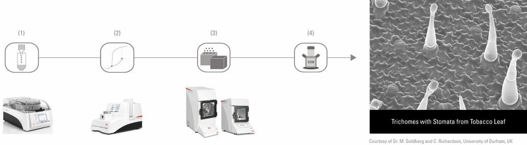
(1) Automated tissue processing (EM TP) | (2) Automated critical point drying (EM CPD300) | (3) Carbon and/or sputter coating (EM ACE200 / EM ACE600) | (4) Image analysis in the SEM. Image Credit: Leica Microsystems-Nanotechnology & EM Sample Preparation-EMEA
SEM/LM Solid State Preparation-Broad Ion Beam Cross Sectioning
Although it can be used for LM investigations, this approach is most frequently used for solid-state SEM samples. When the sample has a specific target that needs to be exposed for observation, the sample must be well-cut to get to the inner structure of the part of interest. After that, non-conductive samples must be coated to make them suitable for SEM observation.
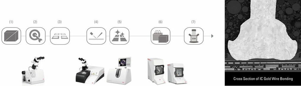
(1)–(3) Cross Sectioning, Target Preparation, Grinding (EM TXP) | (4) & (5) Ion Beam Milling & High End Polishing (EM TIX 3X or EM RES102) | (6) Coating (EM ACE200 / EM ACE600) | (7) SEM Analysis. Image Credit: Leica Microsystems-Nanotechnology & EM Sample Preparation-EMEA
Cryo-SEM Sample Preparation and Transfer-Broad Ion Beam Cross Sectioning
This cryo transfer workflow is used for high-pressure frozen samples, including hard and brittle material (e.g., clay with quartz).
Throughout the entire preparation procedure, which includes high-pressure freezing, mechanical pre-processing using a cryo-saw, an ion beam milling step, and finally, transference to the cryo-SEM, the sample must be kept at a temperature of –150 °C.
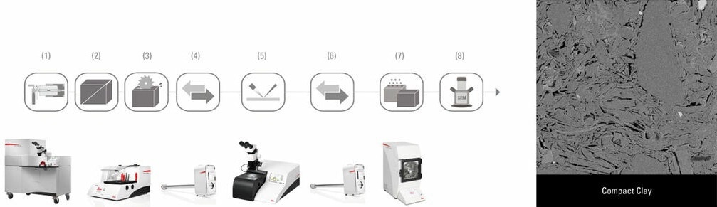
(1) High Pressure Freezing (EM ICE) | (2)–(3) Cross Sectioning & Cutting (EM VCM) | (4) Transfer (EM VCT500) | (5) Ion Beam Milling (EM TIC 3X) | (6) Transfer (EM VCT500) | (7) Coating (EM ACE600) | (8) Cryo-SEM Analysis. Image Credit: Leica Microsystems-Nanotechnology & EM Sample Preparation-EMEA
EM/LM Solid State Preparation-Broad Ion Beam Polishing
This technique is used for large solid-state SEM or LM samples. When a large area (several cm2) of the sample has to be investigated at the highest quality level (e.g., EBSD), the sample is mechanically pre-prepared (with a mirror-like finish) and then finally prepared using the ion beam polishing method.
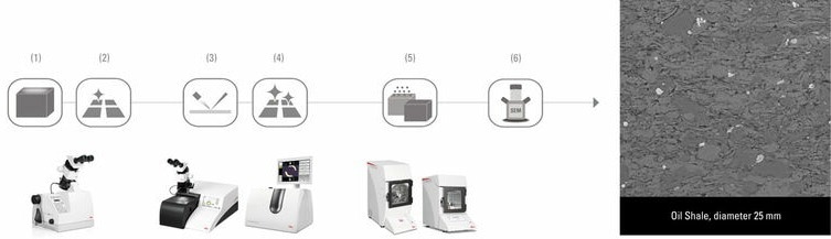
(1) & (2) Surfacing & Polishing (EM TXP) | (3) & (4) Ion Beam Milling & High End Polishing (EM TIC 3X or EM RES102) | (5) Coating (EM ACE200 / EM ACE600) | (6) SEM Analysis. Image Credit: Leica Microsystems-Nanotechnology & EM Sample Preparation-EMEA
Section Tomography 3D Workflow
With this workflow, users can study the interaction and organization of biological structures within a defined 3D volume. The samples must first be processed at room temperature before semi-thick serial sectioning onto TEM grids. After the staining step, TEM imaging should be performed.
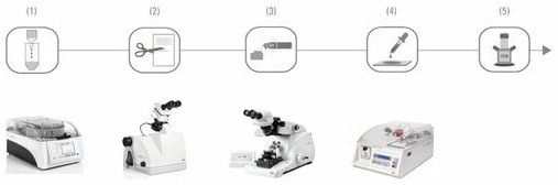
(1) Automated tissue processing (EM TP) | (2) Trimming (EM TRIM2) | (3) Serial sectioning (EM UC7) | (4) Staining (EM AC20) | (5) Image analysis in the TEM. Image Credit: Leica Microsystems-Nanotechnology & EM Sample Preparation-EMEA